|
|
|
PDF NJU7296 Data sheet ( Hoja de datos )
| Número de pieza | NJU7296 | |
| Descripción | SYSTEM RESET IC | |
| Fabricantes | New Japan Radio | |
| Logotipo | ||
Hay una vista previa y un enlace de descarga de NJU7296 (archivo pdf) en la parte inferior de esta página. Total 10 Páginas | ||
|
No Preview Available !
NJU7296
SYSTEM RESET IC WITH DELAY CIRCUIT
■ GENERAL DESCRIPTION
The NJU7296 is a system reset IC with built-in delay circuit that
monitors the status of a power line, and outputs a reset signal to
the microcomputer.
The NJU7296 outputs a reset signal when fall below the detection
voltage.
Delay times are fixed internally and those are set in each of rising
and falling.
It is possible to monitor multiplex power line by combination of
NJU7296 because output voltage VOUT is kept Low level when
EXT Pin is Low level by connecting with other NJU7296.
Detection voltage’s default value is 1.0V. It can be adjusted to
desired voltage by the resistor divider.
In addition, a hysteresis voltage can be set arbitrarily by inserting a
resistor between the VIN pin and the HYS pin.
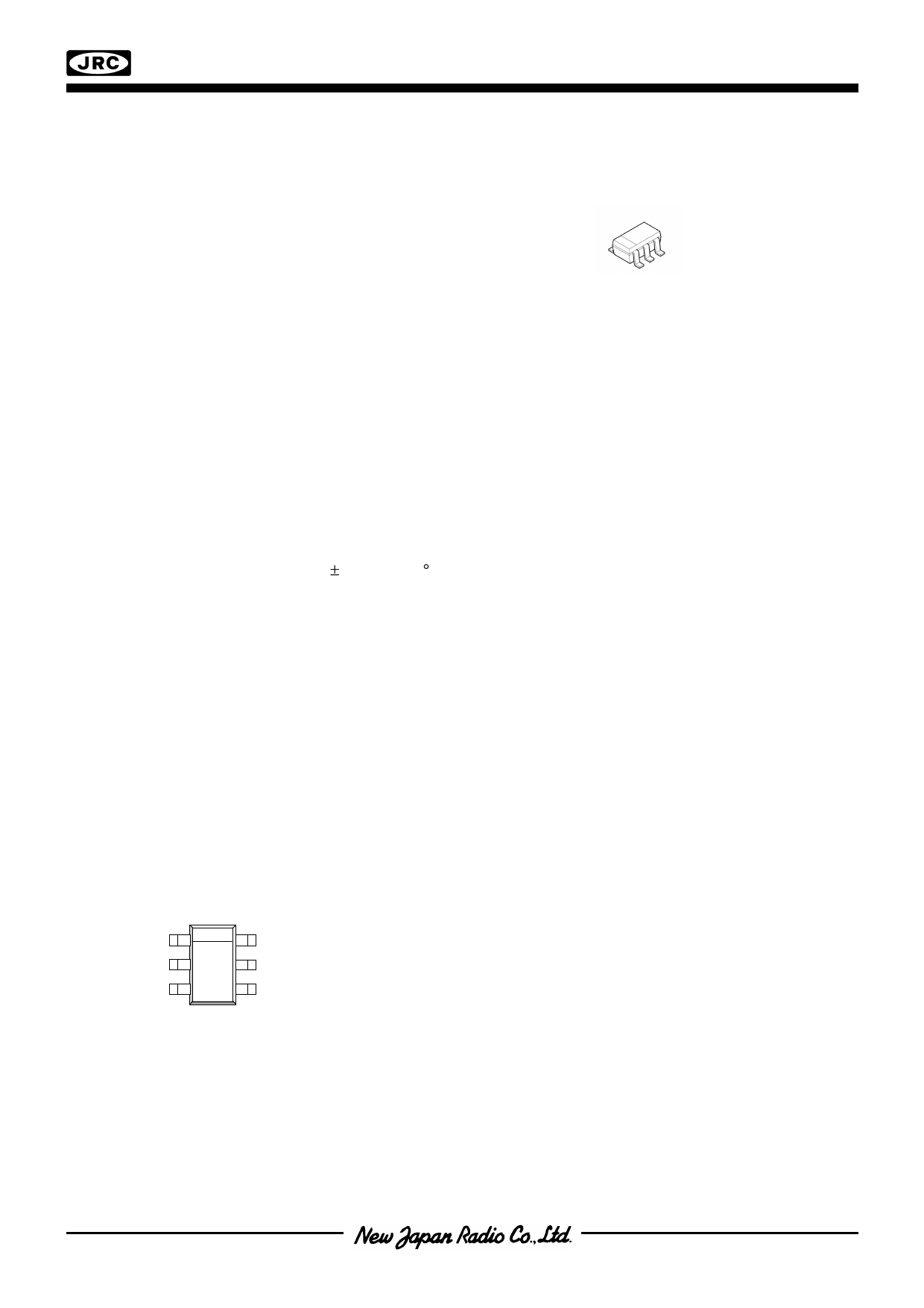
■ PACKAGE OUTLINE
NJU7296F1
■ FEATURES
● High Precision Detection Voltage
● Detection Voltage
● Reset Output Logic
● Delay Circuit (Internal Fixed type)
● Ultra Low Quiescent Current
● Supply Voltage Range
● External Input pin
● Adjustable Hysteresis Voltage
● Output Type
● Package
1.0% (Ta=25 C)
1.0V (default) and adjustable with external resistor
Reset Low output when VIN pin is detection voltage or below
*If required reset low output when VIN pin is detection voltage or more, see the
NJU7295.
Rising / Falling independent setting
1.7µA typ.
1.5 to 5.5V
While inputting low signal, keep output Low level
CMOS output
SOT-23-6-1
■ PIN CONFIGURATION
VIN 1
VSS 2
EXT 3
6 HYS
5 VOUT
4 VDD
Pin Function
1. VIN
2. VSS
3. EXT
:Input Voltage pin
:Ground pin
:External Input pin
4. VDD
5. VOUT
6. HYS
:Supply Voltage pin
:Output pin
:External Resistor pin for setting Hysteresis Voltage
Ver.2016-01-07
-1-
1 page 
■ FUNCTION DESCRIPTION
(1) Basic Operation
Input Voltage
(VIN)
Detection Voltage
(VDET)
VSS
Output Voltage
(VOUT)
VSS
Delay Time1
(td1)
NJU7296
(1) When input voltage VIN falls below the
detection voltage VDET, after the delay time
which is fixed for each version, the output
Release Voltage *
(VDET)
voltage VOUT is switched from High
level to Low level.
*In case of not setting
the hysteresis voltage. (2) In the state of VIN is below the release
voltage VDET, the reset state is maintained.
The default release voltage VDET is same as
detection voltage VDET, although can be set
the hysteresis by inserting a resistor between
the VIN pin and the HYS pin.
Delay Time2
(td2)
(3) When VIN increases and it reaches release
voltage VDET, after the delay time which is
fixed for each version, VOUT is switched from
Low level to High level.
Ver.2016-01-07
-5-
5 Page | ||
| Páginas | Total 10 Páginas | |
| PDF Descargar | [ Datasheet NJU7296.PDF ] | |
Hoja de datos destacado
| Número de pieza | Descripción | Fabricantes |
| NJU7291 | SYSTEM RESET IC | New Japan Radio |
| NJU7295 | SYSTEM RESET IC | New Japan Radio |
| NJU7296 | SYSTEM RESET IC | New Japan Radio |
| Número de pieza | Descripción | Fabricantes |
| SLA6805M | High Voltage 3 phase Motor Driver IC. |
Sanken |
| SDC1742 | 12- and 14-Bit Hybrid Synchro / Resolver-to-Digital Converters. |
Analog Devices |
|
DataSheet.es es una pagina web que funciona como un repositorio de manuales o hoja de datos de muchos de los productos más populares, |
| DataSheet.es | 2020 | Privacy Policy | Contacto | Buscar |