|
|
|
PDF S27KS0641 Data sheet ( Hoja de datos )
| Número de pieza | S27KS0641 | |
| Descripción | Self-Refresh DRAM | |
| Fabricantes | Cypress Semiconductor | |
| Logotipo | ||
Hay una vista previa y un enlace de descarga de S27KS0641 (archivo pdf) en la parte inferior de esta página. Total 29 Páginas | ||
|
No Preview Available !
ADVANCE
S27KL0641, S27KS0641
HyperRAM™ Self-Refresh DRAM
3.0V/1.8V 64 Mb (8 MB)
Distinctive Characteristics
HyperBus™ Low Signal Count Interface
3.0V I/O, 11 bus signals
– Single ended clock (CK)
1.8V I/O, 12 bus signals
– Differential clock (CK, CK#)
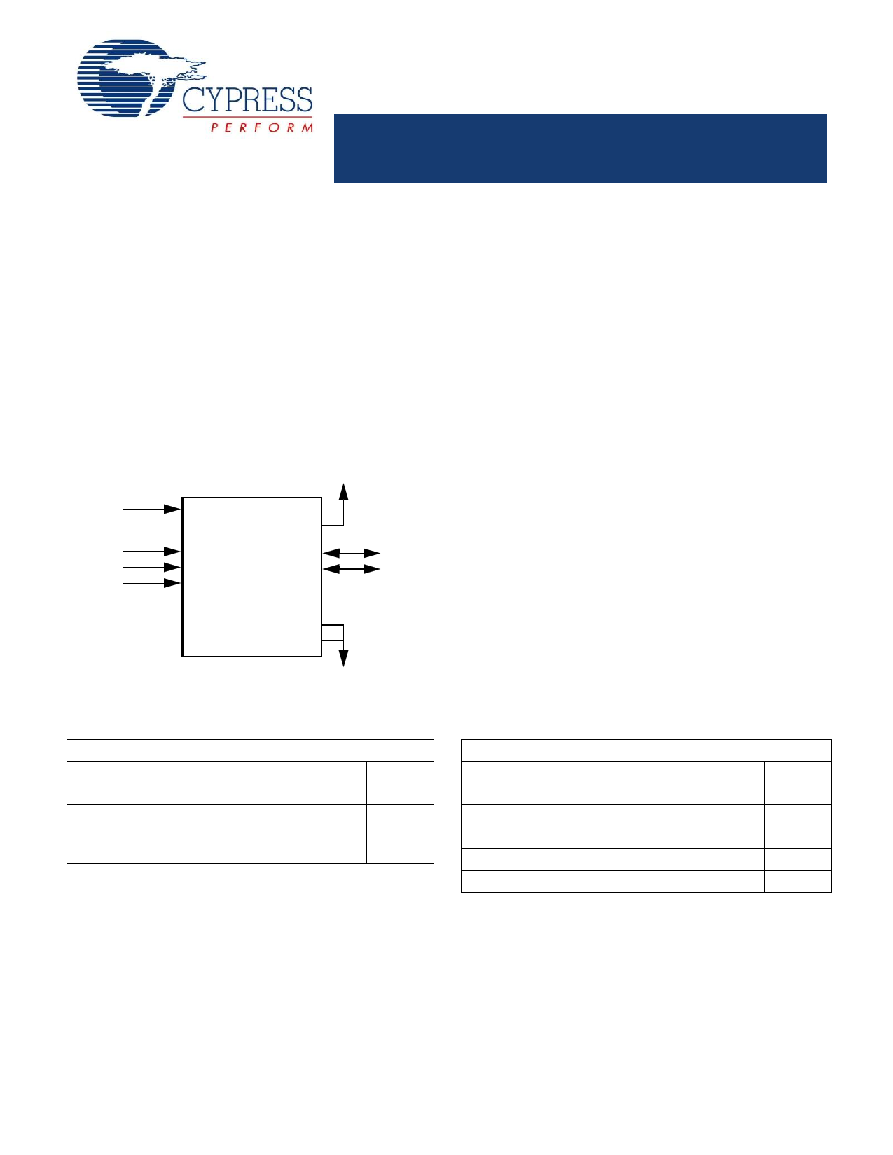
Chip Select (CS#)
8-bit data bus (DQ[7:0])
Read-Write Data Strobe (RWDS)
– Bidirectional Data Strobe / Mask
– Output at the start of all transactions to indicate refresh
latency
– Output during read transactions as Read Data Strobe
– Input during write transactions as Write Data Mask
RESET#
CS#
CK
CK#
VCC
VCCQ
DQ[7:0]
RWDS
High Performance
Up to 333MB/s
Double-Data Rate (DDR) - two data transfers per clock
166-MHz clock rate (333 MB/s) at 1.8V VCC
100-MHz clock rate (200 MB/s) at 3.0V VCC
Sequential burst transactions
Configurable Burst Characteristics
– Wrapped burst lengths:
– 16 bytes (8 clocks)
– 32 bytes (16 clocks)
– 64 bytes (32 clocks)
– 128 bytes (64 clocks)
– Linear burst
– Hybrid option - one wrapped burst followed by linear burst
– Wrapped or linear burst type selected in each transaction
– Configurable output drive strength
Package and Die Options
– 24-ball FBGA footprint
VSS
VSSQ
Performance Summary
Read Transaction Timings
Maximum Clock Rate at 1.8V VCC/VCCQ
Maximum Clock Rate at 3.0V VCC/VCCQ
Maximum Access Time, (tACC at 166 MHz)
Maximum CS# Access Time to first word at
166 MHz (excluding refresh latency)
166 MHz
100 MHz
36 ns
56 ns
Maximum Current Consumption
Burst Read or Write (linear burst at 166 MHz, 1.8V)
Power On Reset
Standby (CS# = High, 3V, 105 °C)
Deep Power Down (CS# = High, 3V, 105 °C)
Standby (CS# = High, 1.8V, 105 °C)
Deep Power Down (CS# = High, 1.8V, 105 °C)
60 mA
50 mA
300 µA
40 µA
300 µA
20 µA
Errata: For information on silicon errata, see "Errata” on page 27. Details include trigger conditions, devices affected, and proposed workaround.
Cypress Semiconductor Corporation • 198 Champion Court
Document Number: 001-97964 Rev. *E
• San Jose, CA 95134-1709 • 408-943-2600
Revised March 01, 2016
1 page 
ADVANCE
S27KL0641, S27KS0641
3. HyperBus Interface
For the general description of how the HyperBus interface operates in HyperRAM memories, refer to the HyperBus specification.
The following section describes HyperRAM device dependent aspects of HyperBus interface operation.
All bus transactions can be classified as either read or write. A bus transaction is started with CS# going Low with CK = Low and
CK# = High. The transaction to be performed is presented to the HyperRAM device during the first three clock cycles in a DDR
manner using all six clock edges. These first three clocks transfer three words of Command / Address (CA0, CA1, CA2) information
to define the transaction characteristics:
Read or write transaction
Whether the transaction will be to the memory array or to register space.
Whether a read transaction will use a linear or wrapped burst sequence
The target half-page address (row and upper order column address)
The target Word (within half-page) address (lower order column address)
Once the transaction has been defined, a number of idle clock cycles are used to satisfy initial read or write access latency
requirements before data is transferred. During the Command-Address portion of all transactions, RWDS is used by the memory to
indicate whether additional initial access latency will be inserted for a required refresh of the memory array.
When data transfer begins, read data is edge aligned with RWDS transitions or write data is center aligned with clock transitions.
During read data transfer, RWDS serves as a source synchronous data timing strobe. During write data transfer, clock transitions
provide the data timing reference and RWDS is used as a data mask. When RWDS is Low during a write data transfer, the data byte
is written into memory; if RWDS is High during the transfer the byte is not written.
Data is transferred as 16-bit values with the first eight bits transferred on a High going CK (write data or CA bits) or RWDS edge
(read data) and the second eight bits being transferred on the Low going CK or RWDS edge. Data transfers during read or write
operations can be ended at any time by bringing CS# High when
CK = Low and CK# = High.
The clock may stop in the idle state while CS# is High.
The clock may also stop in the idle state for short periods while CS# is Low, as long as this does not cause a transaction to exceed
the CS# maximum time low (tCSM) limit. This is referred to as Active Clock Stop mode. In some HyperBus devices this mode is used
for power reduction. However, due to the relatively short tCSM period for completing each data transfer, the Active Clock Stop mode
is generally not useful for power reduction but, may be used for short duration data flow control by the HyperBus master.
3.1 Command-Address Bit Assignments
Table 3.1 Command-Address Bit Definitions
CA Bit#
47
46
45
44-35 (64 Mb)
34-22 (64 Mb)
21-16
Bit Name
R/W#
Address Space
(AS)
Burst Type
Reserved
Row Address
Upper Column
Address
Bit Function
Identifies the transaction as a read or write.
R/W# = 1 indicates a Read transaction
R/W# = 0 indicates a Write transaction
Indicates whether the read or write transaction accesses the memory or register spaces.
AS = 0 indicates memory space.
AS = 1 indicates the register space.
The register space is used to access device ID and Configuration registers.
Indicates whether the burst will be linear or wrapped.
Burst Type = 0 indicates wrapped burst
Burst Type = 1 indicates linear burst
Reserved for future row address expansion.
Reserved bits should be set to 0 by the HyperBus master.
Row component of the target address: System word address bits A23-A9.
Upper Column component of the target address: System word address bits A8-A3.
Document Number: 001-97964 Rev. *E
Page 5 of 29
5 Page 
ADVANCE
S27KL0641, S27KS0641
.
Table 5.6 Example Wrapped Burst Sequences
Burst Selection
CA[45] CR0[2:0]
Burst
Type
Wrap
Start
Boundary Address
(bytes)
(Hex)
Address Sequence (Hex)
(Words)
03, 04, 05, 06, 07, 08, 09, 0A, 0B, 0C, 0D, 0E, 0F, 10, 11, 12, 13, 14, 15,
16, 17, 18, 19, 1A, 1B, 1C, 1D, 1E, 1F, 20, 21, 22, 23, 24, 25, 26, 27, 28,
0
000
Hybrid
128
128 Wrap
29, 2A, 2B, 2C, 2D, 2E, 2F, 30, 31, 32, 33, 34, 35, 36, 37, 38, 39, 3A, 3B,
once then XXXXXX03 3C, 3D, 3E, 3F, 00, 01, 02
Linear
(wrap complete, now linear beyond the end of the initial 128 byte wrap
group)
40, 41, 42, 43, 44, 45, 46, 47, 48, 49, 4A, 4B, 4C, 4D, 4E, 4F, 50, 51, ...
03, 04, 05, 06, 07, 08, 09, 0A, 0B, 0C, 0D, 0E, 0F, 10, 11, 12, 13, 14, 15,
64 Wrap
16, 17, 18, 19, 1A, 1B, 1C, 1D, 1E, 1F, 00, 01, 02,
0 001 Hybrid 64 once then XXXXXX03 (wrap complete, now linear beyond the end of the initial 64 byte wrap
Linear
group)
20, 21, 22, 23, 24, 25, 26, 27, 28, 29, 2A, 2B, 2C, 2D, 2E, 2F, 30, 31, ...
2E, 2F, 30, 31, 32, 33, 34, 35, 36, 37, 38, 39, 3A, 3B, 3C, 3D, 3E, 3F, 20,
64 Wrap
21, 22, 23, 24, 25, 26, 27, 28, 29, 2A, 2B, 2C, 2D,
0 001 Hybrid 64 once then XXXXXX2E (wrap complete, now linear beyond the end of the initial 64 byte wrap
Linear
group)
40, 41, 42, 43, 44, 45, 46, 47, 48, 49, 4A, 4B, 4C, 4D, 4E, 4F, 50, 51, ...
0
010
Hybrid 16
16 Wrap
once then
Linear
02, 03, 04, 05, 06, 07, 00, 01,
XXXXXX02
(wrap complete, now linear beyond the end of the initial 16 byte wrap
group)
08, 09, 0A, 0B, 0C, 0D, 0E, 0F, 10, 11, 12, ...
0
010
Hybrid 16
16 Wrap
once then
Linear
0C, 0D, 0E, 0F, 08, 09, 0A, 0B,
XXXXXX0C
(wrap complete, now linear beyond the end of the initial 16 byte wrap
group)
10, 11, 12, 13, 14, 15, 16, 17, 18, 19, 1A, ...
32 Wrap
0A, 0B, 0C, 0D, 0E, 0F, 00, 01, 02, 03, 04, 05, 06, 07, 08, 09, ...
0 011 Hybrid 32 once then XXXXXX0A
Linear
32 Wrap
1E, 1F, 10, 11, 12, 13, 14, 15, 16, 17, 18, 19, 1A, 1B, 1C, 1D, ...
0 011 Hybrid 32 once then XXXXXX1E
Linear
03, 04, 05, 06, 07, 08, 09, 0A, 0B, 0C, 0D, 0E, 0F, 10, 11, 12, 13, 14, 15,
0 100 Wrap 128 128 XXXXXX03 16, 17, 18, 19, 1A, 1B, 1C, 1D, 1E, 1F, 20, 21, 22, 23, 24, 25, 26, 27, 28,
29, 2A, 2B, 2C, 2D, 2E, 2F, 30, 31, 32, 33, 34, 35, 36, 37, 38, 39, 3A, 3B,
3C, 3D, 3E, 3F, 00, 01, 02, ...
0
101 Wrap 64
64 XXXXXX03 03, 04, 05, 06, 07, 08, 09, 0A, 0B, 0C, 0D, 0E, 0F, 10, 11, 12, 13, 14, 15,
16, 17, 18, 19, 1A, 1B, 1C, 1D, 1E, 1F, 00, 01, 02, ...
0
101 Wrap 64
64 XXXXXX2E 2E, 2F, 30, 31, 32, 33, 34, 35, 36, 37, 38, 39, 3A, 3B, 3C, 3D, 3E, 3F, 20,
21, 22, 23, 24, 25, 26, 27, 28, 29, 2A, 2B, 2C, 2D, ...
0
110 Wrap 16
16 XXXXXX02 02, 03, 04, 05, 06, 07, 00, 01, ...
0
110 Wrap 16
16 XXXXXX0C 0C, 0D, 0E, 0F, 08, 09, 0A, 0B, ...
0
111 Wrap 32
32 XXXXXX0A 0A, 0B, 0C, 0D, 0E, 0F, 00, 01, 02, 03, 04, 05, 06, 07, 08, 09, ...
Document Number: 001-97964 Rev. *E
Page 11 of 29
11 Page | ||
| Páginas | Total 29 Páginas | |
| PDF Descargar | [ Datasheet S27KS0641.PDF ] | |
Hoja de datos destacado
| Número de pieza | Descripción | Fabricantes |
| S27KS0641 | Self-Refresh DRAM | Cypress Semiconductor |
| Número de pieza | Descripción | Fabricantes |
| SLA6805M | High Voltage 3 phase Motor Driver IC. |
Sanken |
| SDC1742 | 12- and 14-Bit Hybrid Synchro / Resolver-to-Digital Converters. |
Analog Devices |
|
DataSheet.es es una pagina web que funciona como un repositorio de manuales o hoja de datos de muchos de los productos más populares, |
| DataSheet.es | 2020 | Privacy Policy | Contacto | Buscar |