|
|
|
PDF CLC407 Data sheet ( Hoja de datos )
| Número de pieza | CLC407 | |
| Descripción | Low-Cost/ Low-Power Programmable Gain Buffer with Disable | |
| Fabricantes | National Semiconductor | |
| Logotipo | ||
Hay una vista previa y un enlace de descarga de CLC407 (archivo pdf) en la parte inferior de esta página. Total 8 Páginas | ||
|
No Preview Available !
August 1996
N
Comlinear CLC407
Low-Cost, Low-Power
Programmable Gain Buffer with Disable
General Description
The Comlinear CLC407 is a low-cost, high-speed (110MHz)
buffer which features user-programmable gains of +2, +1, and -1
V/V. This high-performance part has the added versatility of a
TTL-compatible disable which quickly switches the buffer off in
18ns and back on in 40ns. The CLC407’s high 60mA output
current, coupled with its ultra-low 35mW power consumption
makes it the ideal choice for demanding applications that are
sensitive to both power and cost.
Utilizing Comlinear’s proven architectures, this current feedback
amplifier surpasses the performance of alternate solutions with a
closed-loop design that produces new standards for buffers in
gain accuracy, input impedance, and input bias currents. The
CLC407’s internal feedback network provides an excellent gain
accuracy of 0.1%. High source impedance applications will
benefit from the CLC407’s 6MΩ input impedance along with its
exceptionally low 100nA input bias current.
With 0.1dB flatness to 30MHz and low differential gain and phase
errors, the CLC407 is very useful for professional video process-
ing and distribution. A 110MHz -3dB bandwidth coupled with a
350V/µs slew rate also make the CLC407 a perfect choice in
cost-sensitive applications such as video monitors, fax machines,
copiers, and CATV systems. Back-terminated video applications
will especially appreciate +2 gains which require no external gain
components reducing inventory costs and board space.
Features
s Low-cost
s High output current: 60mA
s High input impedance: 6MΩ
s Gains of +1, +2 with no external components
s Low power: Icc = 3.5mA
s Ultra-fast enable/disable times
s Very low input bias currents: 100nA
s Excellent gain accuracy: 0.1%
s High speed: 110MHz -3dB BW
Applications
s Desktop video systems
s Multiplexers
s Video distribution
s Flash A/D driver
s High-speed switch/driver
s High-source impedance applications
s Peak detector circuits
s Professional video processing
s High resolution monitors
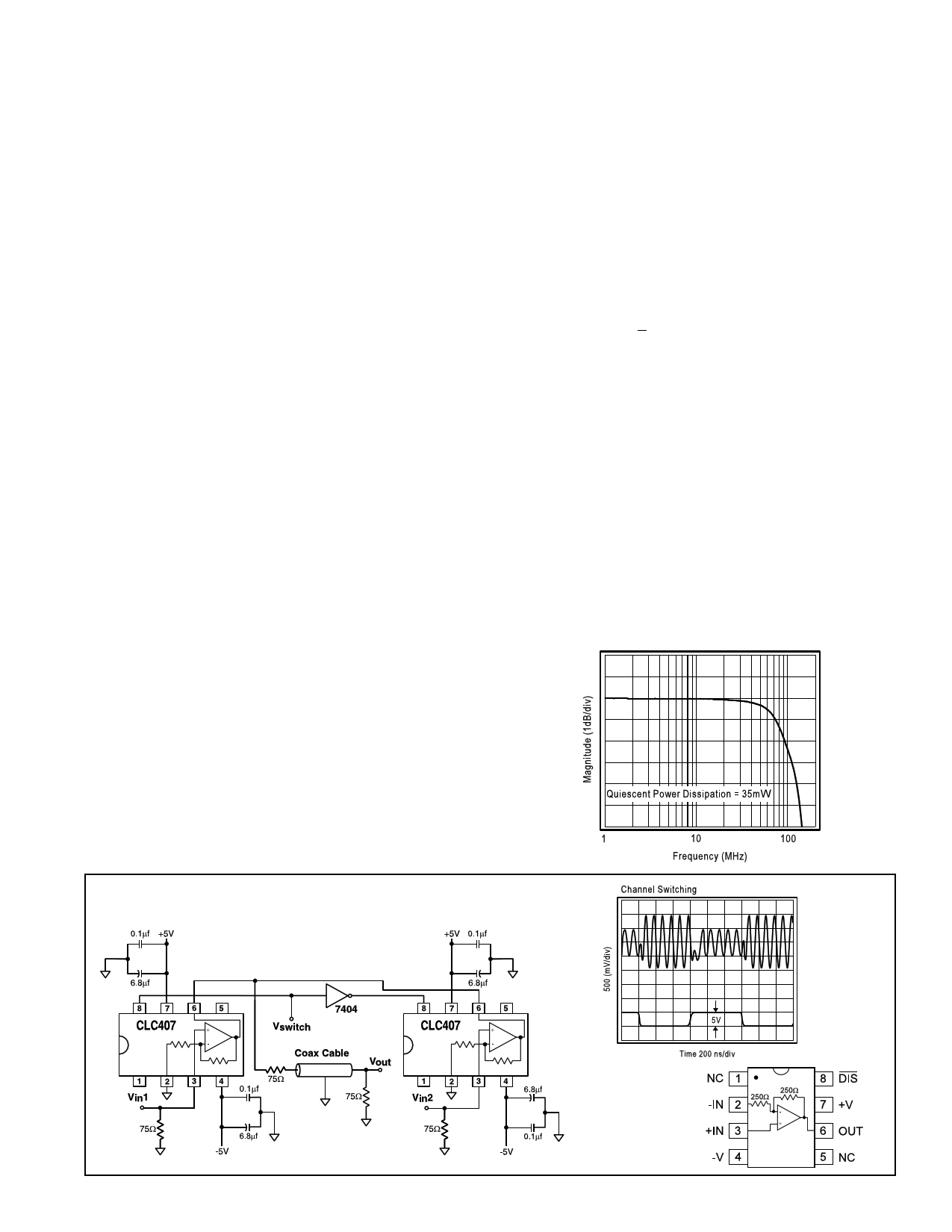
Frequency Response (AV = +2V/V)
Typical Application
2:1 Mux Cable Driver
NOTE: All necessary components are shown.
© 1996 National Semiconductor Corporation
Printed in the U.S.A.
Pinout
DIP & SOIC
http://www.national.com
1 page 
18
SMA
Input
R
Rin
50Ω
27
36
CLC407
45
Rout
50Ω
SMA
Output
Figure 1
Enable/Disable Operation Using +5V Supplies
The CLC407 has a TTL & CMOS logic compatible
disable function. Apply a logic low (i.e. < 0.8V) to pin
8, and the CLC407 is guaranteed disabled across its
temperature range. Apply a logic high to pin 8, (i.e. >
2.0V) and the CLC407 is guaranteed enabled. Voltage,
not current, at pin 8 determines the enable/disable
state of the CLC407.
Disable the CLC407 and its inputs and output become
high impedances. While disabled, the CLC407’s quies-
cent power drops to 8mW.
Use the CLC407’s disable to create analog switches or
multiplexers. Implement a single analog switch with
one CLC407 positioned between an input and output.
Create an analog multiplexer with several CLC407s.
Tie the outputs together and put a different signal on
each CLC407 input.
Operate the CLC407 without connecting pin 8. An
internal 20kΩ pull-up resistor guarantees the CLC407
is enabled when pin 8 is floating.
Enable/Disable Operation for Single or
Unbalanced Supply Operation
Supply 20kΩ
Mid-Point
Bias
Circuitry
20kΩ
Pin 7
+Vcc
Pull-up
Resistor
Vcc -Vee
2
20kΩ
Q2
Q1
I Tail
Pin 8
Disable
CLC407
Pin 4
-Vee
NOTE: Pins 4, 7, 8 are external
Figure 2
Input - Bias Current, Impedances, and Source
Termination Considerations
The CLC407 has:
• a 6MΩ non-inverting input impedance.
• 100nA non-inverting input bias current.
If a large source impedance application is considered,
remove all parasitic capacitance around the non-invert-
ing input and source traces. Parasitic capacitances
near the input and source act as a low-pass filter and
reduce bandwidth.
Current feedback op amps have uncorrelated input
bias currents. These uncorrelated bias currents
prevent source impedance matching on each input
from cancelling offsets. Refer to application note
OA-07 of the data book to find specific circuits to
correct DC offsets.
Layout Considerations
Whenever questions about layout arise, USE THE
EVALUATION BOARD AS A TEMPLATE.
Use the 730013 and 730026 evaluation boards for the
DIP and SOIC respectively. These board layouts were
optimized to produce the typical performance of the
CLC407 shown in the data sheet. To reduce parasitic
capacitances, the ground plane was removed near
pins 2, 3, and 6. To reduce series inductance, trace
lengths of components and nodes were minimized.
Parasitics on traces degrade performance. Minimize
coupling from traces to both power and ground
planes. Use low inductance resistors for leaded
components .
Do not use dip sockets for the CLC407 DIP amplifiers.
These sockets can peak the frequency domain
response or create overshoot in the time domain
response. Use flush-mount socket pins if socketing
cannot be avoided. The 730013 circuit board device
holes are sized for Cambion P/N 450-2598 socket pins
or their functional equivalent.
Insert the back matching resistor Rout shown in
Figure 3 when driving coaxial cable or a capacitive
load. Use the plot in the typical performance section
labeled “Settling Time vs. Capacitive Load” to determine
the optimum resistor value for Rout for different capac-
itive loads. This optimal resistance improves settling
time for pulse-type applications and increases stability.
Figure 2 illustrates the internal enable/disable
operation of the CLC407. When pin 8 is left floating or
is tied to +Vcc, Q1 is on and pulls tail current through
the CLC407 circuitry. When pin 8 is less than 0.8V
above the supply mid-point, Q1 stops tail current from
flowing in the bias circuitry. The CLC407 is now disabled.
Disable Limitations
The internal feedback resistor, Rf limits off isolation in
inverting gain configurations. Do not apply voltages
greater than +Vcc or less than -Vee to pin 8.
5
J1 = 0Ω
1
2
SMA
Input
Rin
50Ω
3
CLC407
4
C2 C4
0.1µfd 6.8µfd
8
7 C1
6 0.1µfd
Rout
5 50Ω
-5V
C3
6.8µfd
+5V
+
SMA
Output
+
Figure 3
http://www.national.com
5 Page | ||
| Páginas | Total 8 Páginas | |
| PDF Descargar | [ Datasheet CLC407.PDF ] | |
Hoja de datos destacado
| Número de pieza | Descripción | Fabricantes |
| CLC40 | Fllstandssensoren Schaltverstarker Baureihe CLC | ETC |
| CLC40-L05 | Fllstandssensoren Schaltverstarker Baureihe CLC | ETC |
| CLC40-L15 | Fllstandssensoren Schaltverstarker Baureihe CLC | ETC |
| CLC40-L50 | Fllstandssensoren Schaltverstarker Baureihe CLC | ETC |
| Número de pieza | Descripción | Fabricantes |
| SLA6805M | High Voltage 3 phase Motor Driver IC. |
Sanken |
| SDC1742 | 12- and 14-Bit Hybrid Synchro / Resolver-to-Digital Converters. |
Analog Devices |
|
DataSheet.es es una pagina web que funciona como un repositorio de manuales o hoja de datos de muchos de los productos más populares, |
| DataSheet.es | 2020 | Privacy Policy | Contacto | Buscar |