|
|
|
PDF 74F657 Data sheet ( Hoja de datos )
| Número de pieza | 74F657 | |
| Descripción | Octal Bidirectional Transceiver | |
| Fabricantes | National Semiconductor | |
| Logotipo | ||
Hay una vista previa y un enlace de descarga de 74F657 (archivo pdf) en la parte inferior de esta página. Total 10 Páginas | ||
|
No Preview Available !
December 1994
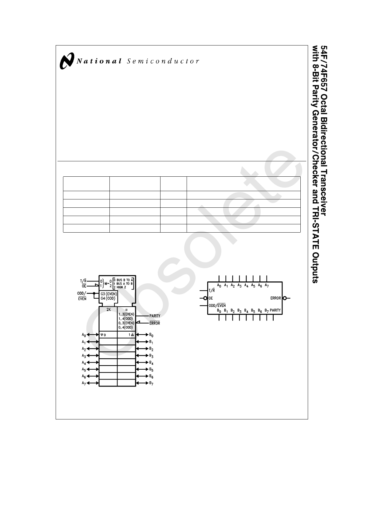
54F 74F657 Octal Bidirectional Transceiver
with 8-Bit Parity Generator Checker
and TRI-STATE Outputs
General Description
The ’F657 contains eight non-inverting buffers with
TRI-STATE outputs and an 8-bit parity generator checker
It is intended for bus-oriented applications The buffers have
a guaranteed current sinking capability of 24 mA (20 mA mil)
at the A port and 64 mA (48 mA mil) at the B port
Features
Y 300 Mil 24-pin slimline DIP
Y Combines ’F245 and ’F280A functions in one package
Y TRI-STATE outputs
Y B Outputs sink 64 mA (48 mA mil)
Y 12 mA source current B side
Y Input diodes for termination effects
Commercial
74F657SPC
75F657SC (Note 1)
Military
54F657SDM (Note 2)
54F657FM (Note 2)
54F657LM (Note 2)
Package
Number
N24C
J24F
M24B
W24C
E28A
Package Description
24-Lead (0 300 Wide) Molded Dual-In-Line
24-Lead (0 300 Wide) Ceramic Dual-In-Line
24-Lead (0 300 Wide) Molded Small Outline JEDEC
24-Lead Cerpack
24-Lead Ceramic Leadless Chip Carrier Type C
Note 1 Devices also available in 13 reel Use suffix e SCX
Note 2 Military grade device with environmental and burn-in processing Use suffix e DMQB FMQB and LMQB
Logic Symbols
IEEE IEC
TL F 9584 – 1
TL F 9584 – 5
TRI-STATE is a registered trademark of National Semiconductor Corporation
C1995 National Semiconductor Corporation TL F 9584
RRD-B30M75 Printed in U S A
1 page 
Absolute Maximum Ratings (Note 1)
If Military Aerospace specified devices are required
please contact the National Semiconductor Sales
Office Distributors for availability and specifications
Storage Temperature
b65 C to a150 C
Ambient Temperature under Bias
b55 C to a125 C
Junction Temperature under Bias
Plastic
VCC Pin Potential to
Ground Pin
b55 C to a175 C
b55 C to a150 C
b0 5V to a7 0V
Input Voltage (Note 2)
b0 5V to a7 0V
Input Current (Note 2)
b30 mA to a5 0 mA
Voltage Applied to Output
in HIGH State (with VCC e 0V)
Standard Output
TRI-STATE Output
b0 5V to VCC
b0 5V to a5 5V
DC Electrical Characteristics
Current Applied to Output
in LOW State (Max)
twice the rated IOL (mA)
Note 1 Absolute maximum ratings are values beyond which the device may
be damaged or have its useful life impaired Functional operation under
these conditions is not implied
Note 2 Either voltage limit or current limit is sufficient to protect inputs
Recommended Operating
Conditions
Free Air Ambient Temperature
Military
Commercial
b55 C to a125 C
0 C to a70 C
Supply Voltage
Military
Commercial
a4 5V to a5 5V
a4 5V to a5 5V
Symbol
VIH
VIL
VCD
VOH
VOL
IIH
IBVI
IBVIT
IIL
IOZH
IOZL
IIH a IOZH
IIL a IOZL
IOS
ICEX
IZZ
ICCH
ICCL
ICCZ
Parameter
Input HIGH Voltage
Input LOW Voltage
Input Clamp Diode Voltage
Output HIGH
Voltage
54F 10%VCC
54F 10% VCC
54F 10% VCC
74F 10% VCC
74F 10% VCC
74F 10% VCC
74F 5% VCC
74F 5% VCC
Output LOW
Voltage
54F 10% VCC
54F 10% VCC
74F 10% VCC
74F 10% VCC
Input HIGH Current
Input HIGH Current
Breakdown Test
Input HIGH Current
Breakdown Test (I O)
Input LOW Current
Output Leakage Current
Output Leakage Current
Output Leakage Current
Output Leakage Current
Output Short-Circuit Current
Output HIGH Leakage
Current
Bus Drainage Test
Power Supply Current
Power Supply Current
Power Supply Current
54F 74F
Min Typ Max
20
08
b1 2
25
24
20
25
24
20
27
27
05
0 55
05
0 55
20
40
100
10
20
b20
b40
50
b50
70
90
b70
b90
b60
b100
b150
b225
250
10
20
500
101 125
112 150
109 145
Units
V
V
V
V
V
mA
mA
mA
mA
mA
mA
mA
mA
mA
mA
mA
mA
mA
mA
mA
mA
VCC
Min
Min
Min
Max
VCC e 0
Max
Max
Max
Max
Max
Max
Max
Max
Max
Max
0 0V
Max
Max
Max
Conditions
Recognized as a HIGH Signal
Recognized as a LOW Signal
IIN e b18 mA
IOH e b1 mA (An)
IOH e b3 mA (An Bn Parity ERROR)
IOH e b12 mA (Bn Parity ERROR)
IOH e b1 mA (An)
IOH e b3 mA (An Bn Parity ERROR)
IOH e b15 mA (Bn Parity ERROR)
IOH e b1 mA (An)
IOH e b3 mA (An Bn Parity ERROR)
IOL e 20 mA (An)
IOL e 48 mA (Bn Parity ERROR)
IOL e 24 mA (An)
IOL e 64 mA (Bn Parity ERROR)
VIN e 2 7V (ODD EVEN)
VIN 2 7V (T R OE)
VIN e 7 0V (T R OE ODD EVEN)
VIN e 5 5V (Parity Bn)
VIN e 5 5V (An)
VIN e 0 5V (ODD EVEN)
VIN e 0 5V (T R OE)
VOUT e 2 7V (ERROR)
VOUT e 0 5V (ERROR)
VI O e 2 7V (Bn Parity)
VI O e 2 7V (An)
VI O e 0 5V (Bn Parity)
VI O e 0 5V (An)
VOUT e 0V (An)
VOUT e 0V (Bn Parity ERROR)
VOUT e VCC (ERROR)
VOUT e VCC (Bn Parity)
VOUT e VCC (An)
VOUT e 5 25V (An Bn Parity ERROR)
VO e HIGH
VO e LOW
VO e HIGH Z
5
5 Page | ||
| Páginas | Total 10 Páginas | |
| PDF Descargar | [ Datasheet 74F657.PDF ] | |
Hoja de datos destacado
| Número de pieza | Descripción | Fabricantes |
| 74F651 | Transceivers/Registers | Fairchild |
| 74F651 | Transceivers/Registers | National |
| 74F651 | Transceivers and Registers (Rev. A) | Texas Instruments |
| 74F651A | Transceivers/registers | Philips |
| Número de pieza | Descripción | Fabricantes |
| SLA6805M | High Voltage 3 phase Motor Driver IC. |
Sanken |
| SDC1742 | 12- and 14-Bit Hybrid Synchro / Resolver-to-Digital Converters. |
Analog Devices |
|
DataSheet.es es una pagina web que funciona como un repositorio de manuales o hoja de datos de muchos de los productos más populares, |
| DataSheet.es | 2020 | Privacy Policy | Contacto | Buscar |