|
|
|
PDF CDP1822C Data sheet ( Hoja de datos )
| Número de pieza | CDP1822C | |
| Descripción | High-Reliability CMOS 256-Word x 4-Bit LSI Static RAM | |
| Fabricantes | Intersil Corporation | |
| Logotipo | ||
Hay una vista previa y un enlace de descarga de CDP1822C (archivo pdf) en la parte inferior de esta página. Total 5 Páginas | ||
|
No Preview Available !
CDP1822C/3
March 1997
High-Reliability CMOS
256-Word x 4-Bit LSI Static RAM
Features
Description
• For Applications in Aerospace, Military, and Critical
Industrial Equipment
• Interfaces Directly with CDP1802 Microprocessor
• Very Low Operating Current
- At VDD = 5V and Cycle Time = 1µs . . . . . . 4mA (Typ)
• Static CMOS Silicon-On-Sapphire Circuitry
- CD4000 Series Compatible
• Industry Standard Pinout
• Two Chip Select Inputs - Simple Memory Expansion
• Memory Retention for Standby. . . . . . . . . . . . . 2V (Min)
Battery Voltage
• Single Power Supply Operation . . . . . . . . . . 4V to 6.5V
• High Noise Immunity 30% of VDD. . . . . . . . . 4V to 6.5V
• Output Disable for Common I/O Systems
• Three-State Data Output for Bus Oriented Systems
The CDP1822C/3 is a 256 word by 4-bit random access
memory designed for use in memory systems where high
speed, low operating current, and simplicity in use are
desirable. The CDP1822 features high speed and excellent
noise immunity. It has separate data inputs and outputs and
utilizes a single power supply of 4V to 6.5V.
Two Chip Select inputs simplify system expansion. An output
Disable control provides Wire-OR-capability and is also
useful in common Input/Output systems. The Output Disable
input allows this RAM to be used in common data Input/Out-
put systems by forcing the output into a high impedance
state during a write operation independent of the Chip Select
input condition. The output assumes a high impedance state
when the Output Disable is at high level or when the chip is
deselected by CS1 and/or CS2.
The high noise immunity of the CMOS technology is
preserved in this design. For TTL interfacing at 5V operation,
excellent system noise margin is preserved by using an
external pull-up resistor at each input.
• Separate Data Inputs and Outputs
• Latch-Up-Free Transient Radiation Tolerance
Ordering Information
PACKAGE
SBDIP
TEMP. RANGE
-55oC to +125oC
PART
NUMBER
CDP1822CD3
PKG. NO.
D22.4A
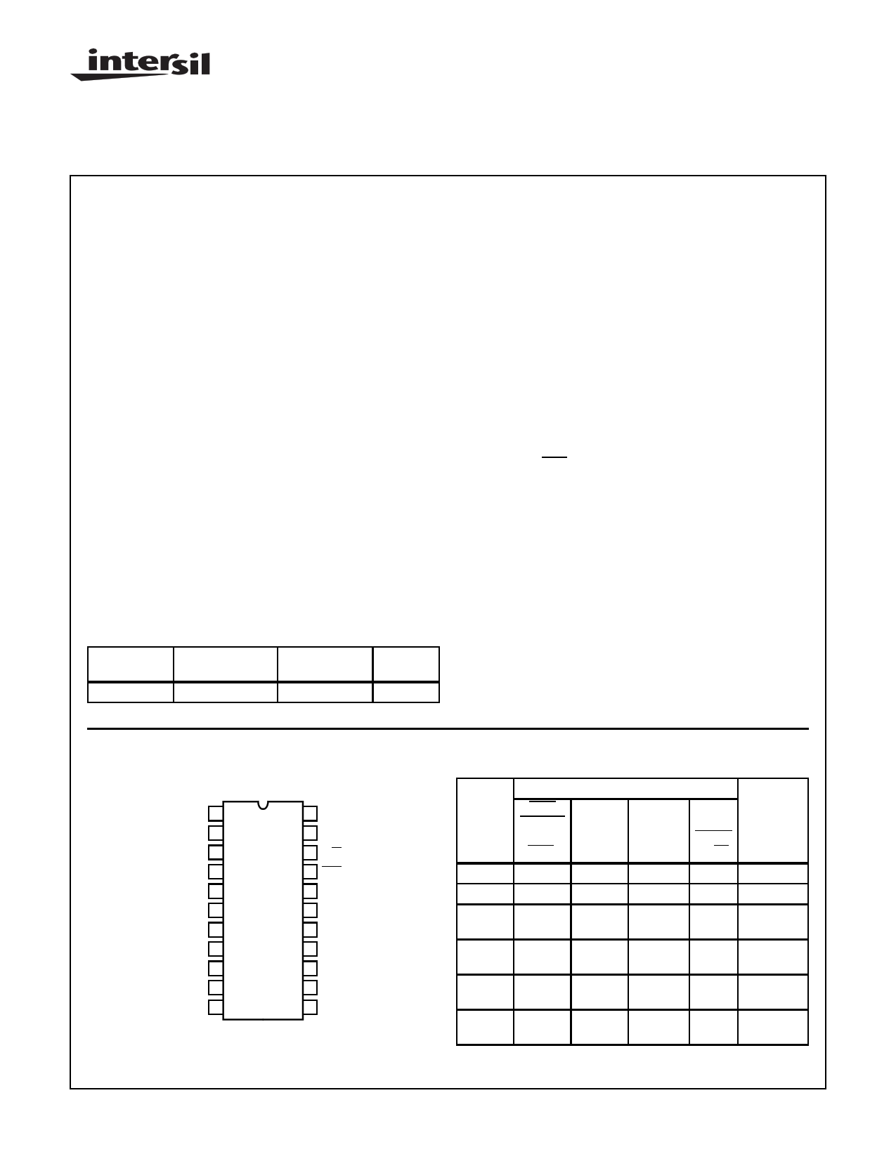
Pinout
CDP1822C/3 (SBDIP)
TOP VIEW
A3 1
A2 2
A1 3
A0 4
A5 5
A6 6
A7 7
VSS 8
DI1 9
DO1 10
DI2 11
22 VDD
21 A4
20 R/W
19 CS1
18 O. D.
17 CS2
16 DO4
15 DI4
14 DO3
13 DI3
12 DO2
OPERATIONAL MODES
INPUTS
MODE
CHIP
SELECT
1
(CS1)
CHIP
SELECT
2
(CS2)
OUTPUT
DISABLE
(OD)
READ/
WRITE
(R/W)
OUTPUT
Read
0
1
0 1 Read
Write
0
1
0 0 Data In
Write
0
1
1 0 High
Impedance
Standby
1
X
X X High
Impedance
Standby
X
0
X X High
Impedance
Output
Disable
X
X
1 X High
Impedance
Logic 1 = High, Logic 0 = Low, X = Don’t Care
CAUTION: These devices are sensitive to electrostatic discharge; follow proper IC Handling Procedures.
http://www.intersil.com or 407-727-9207 | Copyright © Intersil Corporation 1999
6-19
File Number 2981.1
1 page 
CDP1822C/3
Data Retention Specifications
PARAMETER
SYMBOL
TEST
CONDITIONS
VDR
(V)
VDD
(V)
LIMITS
+25oC, -55oC
+125oC
MIN MAX MIN MAX
UNITS
Minimum Data Retention Voltage
(Note 1)
VDR - - - 2 - 2.5 V
Data Retention Quiescent Current IDD 2 - - 70 - 380 µA
(Note 1)
Chip Deselect to Data Retention Time
tCDR
-
5 450 - 650 -
ns
- 10
Recovery to Normal Operation Time
tRC
5 5 450 - 650 - ns
NOTE:
1. Limits designate 100% testing. All other limits are designer’s parameters under given test conditions and do not represent 100% testing.
VDD
CS2
tCDR
DATA RETENTION
MODE
0.95 VDD
0.95 VDD
VDR
tF tR
VIH
VIL
tRC
VIH
VIL
FIGURE 4. LOW VDD DATA RETENTION TIMING WAVEFORMS
VDD
A3
A2
A1
A0
A5
A6
A7
R A8
2kΩ
A8
1
2
3
4
5
6
7
8
9
10
11
R = 2kΩ ±20%
22 VDD
21 A4
20 01
19 A9
18 A11
17 A10
R
16 VDD
15 A8 2kΩ
R
14 VDD
13 A8 2kΩ
R
12 VDD
2kΩ
PACKAGE
D
TEMPERATURE
125oC
DURATION
160 Hrs
VDD
7V
0
01
A0
A1
1.6 2.2 5.0
6.8 7.2
10.0µs
VDD
0
VDD
0
VDD
0
FIGURE 5. DYNAMIC/OPERATING BURN-IN CIRCUIT AND TIMING DIAGRAM
All Intersil semiconductor products are manufactured, assembled and tested under ISO9000 quality systems certification.
Intersil products are sold by description only. Intersil Corporation reserves the right to make changes in circuit design and/or specifications at any time without
notice. Accordingly, the reader is cautioned to verify that data sheets are current before placing orders. Information furnished by Intersil is believed to be accurate
and reliable. However, no responsibility is assumed by Intersil or its subsidiaries for its use; nor for any infringements of patents or other rights of third parties which
may result from its use. No license is granted by implication or otherwise under any patent or patent rights of Intersil or its subsidiaries.
For information regarding Intersil Corporation and its products, see web site http://www.intersil.com
6-23
5 Page | ||
| Páginas | Total 5 Páginas | |
| PDF Descargar | [ Datasheet CDP1822C.PDF ] | |
Hoja de datos destacado
| Número de pieza | Descripción | Fabricantes |
| CDP1822 | 256-Word x 4-Bit LSI Static RAM | Intersil Corporation |
| CDP1822 | 256-Word by 4-Bit LSI Static Random-Access Memory | GE |
| CDP1822C | High-Reliability CMOS 256-Word x 4-Bit LSI Static RAM | Intersil Corporation |
| CDP1822C | 256-Word by 4-Bit LSI Static Random-Access Memory | GE |
| Número de pieza | Descripción | Fabricantes |
| SLA6805M | High Voltage 3 phase Motor Driver IC. |
Sanken |
| SDC1742 | 12- and 14-Bit Hybrid Synchro / Resolver-to-Digital Converters. |
Analog Devices |
|
DataSheet.es es una pagina web que funciona como un repositorio de manuales o hoja de datos de muchos de los productos más populares, |
| DataSheet.es | 2020 | Privacy Policy | Contacto | Buscar |