|
|
|
PDF CDP1877 Data sheet ( Hoja de datos )
| Número de pieza | CDP1877 | |
| Descripción | Programmable Interrupt Controller (PIC) | |
| Fabricantes | Intersil Corporation | |
| Logotipo | ||
Hay una vista previa y un enlace de descarga de CDP1877 (archivo pdf) en la parte inferior de esta página. Total 10 Páginas | ||
|
No Preview Available !
CDP1877,
CDP1877C
March 1997
Programmable Interrupt Controller (PIC)
Features
• Compatible with CDP1800 Series
• Programmable Long Branch Vector Address and
Vector Interval
• 8 Levels of Interrupt Per Chip
• Easily Expandable
• Latched Interrupt Requests
• Hard Wired Interrupt Priorities
• Memory Mapped
• Multiple Chip Select Inputs to Minimize Address
Space Requirements
Ordering Information
TEMP.
PACKAGE RANGE
5V
PKG.
10V NO.
PDIP
-40oC to CDP1877CE CDP1877E E28.6
+85oC
Description
The CDP1877 and CDP1877C are programmable 8-level interrupt control-
lers designed for use in CDP1800 series microprocessor systems. They
provide added versatility by extending the number of permissible interrupts
from 1 to N in increments of 8.
When a high to low transition occurs on any of the PIC interrupt lines (IR0 to
IR7), it will be latched and, unless the request is masked, it will cause the
INTERRUPT line on the PIC and consequently the INTERRUPT input on
the CPU to go low.
The CPU accesses the PIC by having interrupt vector register R(1) loaded
with the memory address of the PIC. After the interrupt S3 cycle, this regis-
ter value will appear at the CPU address bus, causing the CPU to fetch an
instruction from the PIC. This fetch cycle clears the interrupt request latch
bit to accept a new high-to-low transition, and also causes the PIC to issue a
long branch instruction (CO) followed by the preprogrammed vector address
written into the PIC’s address registers, causing the CPU to branch to the
address corresponding to the highest priority active interrupt request.
If no other unmasked interrupts are pending, the INTERRUPT output of the
PIC will return high. When an interrupt is requested on a masked interrupt
line, it will be latched but it will not cause the PIC INTERRUPT output to go
low. All pending interrupts, masked and unmasked, will be indicated by a “1”
in the corresponding bit of the status register. Reading of the status register
will clear all pending interrupt request latches.
Several PICs can be cascaded together by connecting the INTERRUPT out-
put of one chip to the CASCADE input of another. Each cascaded PIC pro-
vides 8 additional interrupt levels to the system. The number of units
cascadable depends on the amount of memory space and the extent of the
address decoding in the system.
Interrupts are prioritized in descending order; IR7 has the highest and IR0
has the lowest priority.
The CDP1877 and CDP1877C are functionally identical. They differ in that
the CDP1877 has a recommended operating voltage range of 4V to 10.5V,
and the CDP1877C has a recommended operating voltage range of 4V to
6.5V.
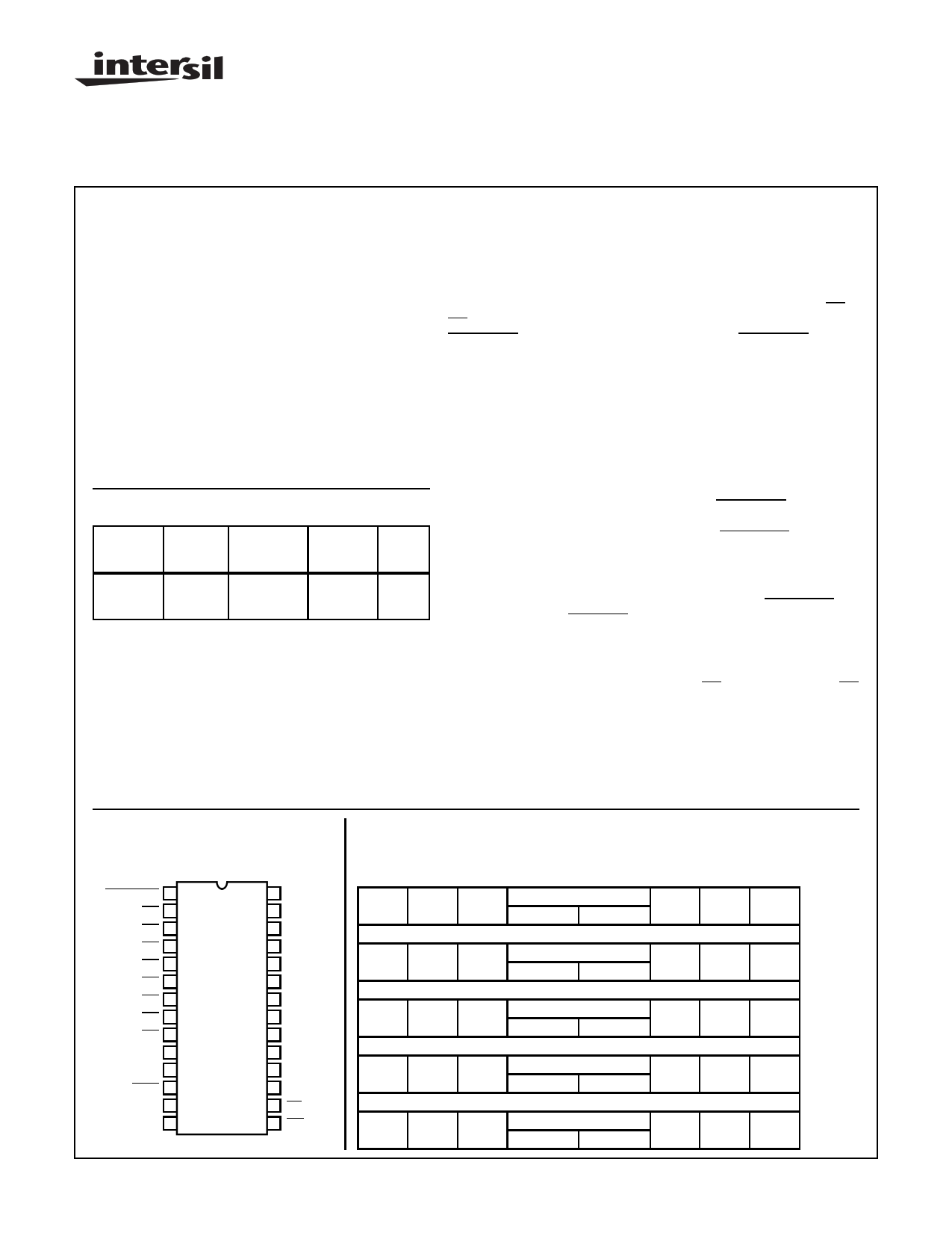
Pinout
CDP1877, CDP1877C (PDIP)
TOP VIEW
CASCADE 1
IR7 2
IR6 3
IR5 4
IR4 5
IR3 6
IR2 7
IR1 8
IR0 9
TPA 10
TPB 11
MWR 12
MRD 13
VSS 14
28 VDD
27 BUS 7
26 BUS 6
25 BUS 5
24 BUS 4
23 BUS 3
22 BUS 2
21 BUS 1
20 BUS 0
19 CS/Ax
18 CS/Ay
17 CS
16 CS
15 INT
Programming Model
PROGRAMMABLE INTERRUPT CONTROLLER (PIC)
BUS 7
A15 A14
BUS 7
B7
BUS 7
B6
M7
BUS 7
M6
S7
BUS 7
S6
P7 P6
PAGE REGISTER
A13 A12
A11 A10
CONTROL REGISTER
B5 B4
B3 B2
MASK REGISTER
M5 M4
M3 M2
STATUS REGISTER
S5 S4
S3 S2
POLLING REGISTER
P5 P4
P3 P2
BUS 0
WRITE
A9 A8 ONLY
BUS 0
WRITE
B1 B0 ONLY
BUS 0
WRITE
M1 M0 ONLY
BUS 0
READ
S1 S0 ONLY
BUS 0
READ
P1 P0 ONLY
CAUTION: These devices are sensitive to electrostatic discharge; follow proper IC Handling Procedures.
http://www.intersil.com or 407-727-9207 | Copyright © Intersil Corporation 1999
4-82
File Number 1319.2
1 page 
CDP1877, CDP1877C
The Low Order Vector Address will be set according to the table below:
LOW ADDRESS BITS
INTERVAL SELECTED NO. OF BYTES
BIT B7
BIT B6
BIT B5
2
SETS A7
SETS A6
SETS A5
4
SETS A7
SETS A6
SETS A5
8
SETS A7
SETS A6
X
16
SETS A7
X
X
NOTES:
1. X = Don’t Care
2. All Don’t Care addresses and addresses A0-A3 are determined by interrupt request.
Mask Register
A ”1” written into any location in this write only register will
mask the corresponding interrupt request line. All interrupt
inputs (except CASCADE) are maskable.
BUS 7
M7
M6
MASK REGISTER BITS
M5 M4 M3
Status Register
In this read only register a “1” will be present in the
corresponding bit location for every masked or unmasked
pending interrupt.
M2
BUS 0
M1 M0
BUS 7
S7
S6
STATUS REGISTER BITS
S5 S4 S3
Polling Register
This read only register provides the low order vector address
and is used to identify the source of interrupt if a polling
technique, rather than interrupt servicing, is used.
S2
BUS 0
S1 S0
BUS 7
P7
P6
POLLING REGISTER BITS
P5 P4 P3 P2
BUS 0
P1 P0
BIT B4
SET A4
X
X
X
WRITE ONLY
READ ONLY
READ ONLY
RESPONSE TO INTERRUPT (AFTER S3 CYCLE)
The PIC’s response to interrogation by the CPU is always 3
bytes long, placed on the data bus in consecutive bytes in
the following format:
First (Instruction) Byte:
LONG BRANCH INSTRUCTION - CO (Hex)
BUS 7
BUS 0
11000000
4-86
5 Page | ||
| Páginas | Total 10 Páginas | |
| PDF Descargar | [ Datasheet CDP1877.PDF ] | |
Hoja de datos destacado
| Número de pieza | Descripción | Fabricantes |
| CDP1870C | (CDP1869C - CDP1876C) Video Interface System | ETC |
| CDP1871 | CMOS Keyboard Encoder | Intersil Corporation |
| CDP1871A | CMOS Keyboard Encoder | GE |
| CDP1871A | CMOS Keyboard Encoder | Intersil Corporation |
| Número de pieza | Descripción | Fabricantes |
| SLA6805M | High Voltage 3 phase Motor Driver IC. |
Sanken |
| SDC1742 | 12- and 14-Bit Hybrid Synchro / Resolver-to-Digital Converters. |
Analog Devices |
|
DataSheet.es es una pagina web que funciona como un repositorio de manuales o hoja de datos de muchos de los productos más populares, |
| DataSheet.es | 2020 | Privacy Policy | Contacto | Buscar |