|
|
|
PDF NCP103 Data sheet ( Hoja de datos )
| Número de pieza | NCP103 | |
| Descripción | 150 mA CMOS Low Dropout Regulator | |
| Fabricantes | ON Semiconductor | |
| Logotipo | ||
Hay una vista previa y un enlace de descarga de NCP103 (archivo pdf) en la parte inferior de esta página. Total 15 Páginas | ||
|
No Preview Available !
NCP103
150 mA CMOS Low Dropout
Regulator
The NCP103 is 150 mA LDO that provides the engineer with a very
stable, accurate voltage with low noise suitable for space constrained,
noise sensitive applications. In order to optimize performance for
battery operated portable applications, the NCP103 employs the
dynamic quiescent current adjustment for very low IQ consumption at
no−load.
Features
• Operating Input Voltage Range: 1.7 V to 5.5 V
• Available in Fixed Voltage Options: 0.9 V to 3.5 V
Contact Factory for Other Voltage Options
• Very Low Quiescent Current of Typ. 50 mA
• Standby Current Consumption: Typ. 0.1 mA
• Low Dropout: 75 mV Typical at 150 mA
• ±1% Accuracy at Room Temperature
• High Power Supply Ripple Rejection: 75 dB at 1 kHz
• Thermal Shutdown and Current Limit Protections
• Stable with a 1 mF Ceramic Output Capacitor
• Available in uDFN 1.0 x 1.0 mm Package
• These Devices are Pb−Free, Halogen Free/BFR Free and are RoHS
Compliant
Typical Applicaitons
• PDAs, Mobile phones, GPS, Smartphones
• Wireless Handsets, Wireless LAN, Bluetooth®, Zigbee®
• Portable Medical Equipment
• Other Battery Powered Applications
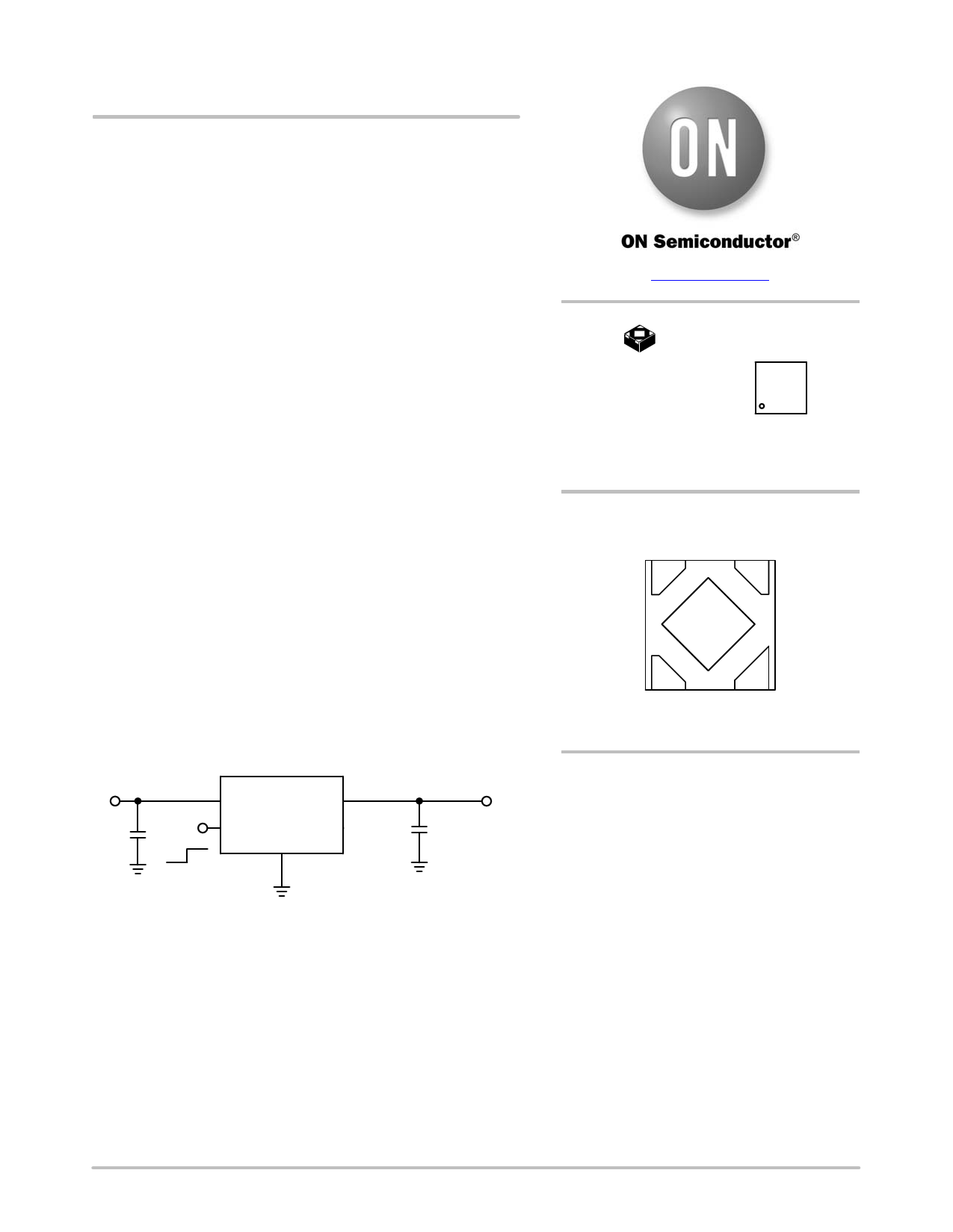
VIN
CIN
IN
ON
OFF
EN
NCP103
OUT
GND
VOUT
COUT
1 mF
Ceramic
www.onsemi.com
1
UDFN4
MX SUFFIX
CASE 517CU
MARKING
DIAGRAM
XX M
1
XX = Specific Device Code
M = Date Code
PIN CONNECTION
EN IN
34
2
GND
1
OUT
(Bottom View)
ORDERING INFORMATION
See detailed ordering, marking and shipping information on
page 14 of this data sheet.
Figure 1. Typical Application Schematic
© Semiconductor Components Industries, LLC, 2016
September, 2016 − Rev. 11
1
Publication Order Number:
NCP103/D
1 page 
NCP103
TYPICAL CHARACTERISTICS
0.1
0.08
0.06
0.04
0.02
0
−0.02
−0.04
−0.06
−0.08
−0.1
VIN = 3.8 V to 5.5 V
VOUT = 2.8 V
IOUT = 1 mA
CIN = 1 mF
COUT = 1 mF
−40 −30 −20 −10 0 10 20 30 40 50 60 70 80 90
TJ, JUNCTION TEMPERATURE (°C)
Figure 9. Line Regulation vs. Temperature
VOUT = 2.8 V
10
9
8
7
6
5
4 VIN = 2.5 V
3 VOUT = 1.2 V
2 IOUT = 1 mA to 150 mA
CIN = 1 mF
1 COUT = 1 mF
0
−40 −30 −20 −10 0 10 20 30 40 50 60 70 80 90
TJ, JUNCTION TEMPERATURE (°C)
Figure 10. Load Regulation vs. Temperature
VOUT = 1.2 V
10
9
8
7
6
5
4
3
VIN = 3.8 V
VOUT = 2.8 V
2 IOUT = 1 mA to 150 mA
1 CIN = 1 mF
COUT = 1 mF
0
−40 −30 −20 −10 0 10 20 30 40 50 60 70 80 90
TJ, JUNCTION TEMPERATURE (°C)
Figure 11. Load Regulation vs. Temperature
VOUT = 2.8 V
100
90
80
70
60
TJ = 85°C
50
40 TJ = −40°C
30
20
10 TJ = 25°C
0
VIN = 3.8 V
VOUT = 2.8 V
CIN = 1 mF
COUT = 1 mF
0 15 30 45 60 75 90 105 120 135 150
IOUT, OUTPUT CURRENT (mA)
Figure 12. Dropout Voltage vs. Output Current
VOUT = 2.8 V
100
90
80 IOUT = 150 mA
70
60 IOUT = 100 mA
50
40
30 IOUT = 0 mA
VIN = 3.8 V
20 VOUT = 2.8 V
10 CIN = 1 mF
0 COUT = 1 mF
−40 −30 −20 −10 0 10 20 30 40 50 60 70 80 90
TJ, JUNCTION TEMPERATURE (°C)
Figure 13. Dropout Voltage vs. Temperature
800
750
700
650 VOUT = 2.8 V
600
550 VOUT = 1.2 V
500
450 VIN = VOUT(nom) + 1 V or 2.5 V
400 VOUT = 90% VOUT(nom)
350 CIN = 1 mF
COUT = 1 mF
300
−40 −30 −20 −10 0 10 20 30 40 50 60 70 80 90
TJ, JUNCTION TEMPERATURE (°C)
Figure 14. Current Limit vs. Temperature
www.onsemi.com
5
5 Page 
IOUT
NCP103
TYPICAL CHARACTERISTICS
tRISE = 1 ms
VIN = 3.8 V
VOUT = 2.8 V
CIN = 1 mF (MLCC)
COUT = 1 mF (MLCC)
IOUT
tFALL = 1 ms
VIN = 3.8 V
VOUT = 2.8 V
CIN = 1 mF (MLCC)
COUT = 1 mF (MLCC)
VOUT
VIN = 5.5 V
VIN = 3.8 V
2 ms/div
Figure 38. Load Transient Response − Rising
Edge, VOUT = 2.8 V, IOUT = 1 mA to 150 mA,
VIN = 3.8 V, 5.5 V
VIN
VOUT
VIN = 5.5 V
VOUT = 2.8 V
IOUT = 10 mA
CIN = 1 mF (MLCC)
COUT = 1 mF (MLCC)
4 ms/div
Figure 40. Turn−on/off − Slow Rising VIN
VOUT
VIN = 3.8 V
VIN = 5.5 V
10 ms/div
Figure 39. Load Transient Response − Falling
Edge, VOUT = 2.8 V, IOUT = 1 mA to 150 mA,
VIN = 3.8 V, 5.5 V
Overheating
Full Load
IOUT
Thermal Shutdown
VOUT
VIN = 5.5 V
VOUT = 1.2 V
CIN = 1 mF (MLCC)
COUT = 1 mF (MLCC)
TSD Cycling
10 ms/div
Figure 41. Short−Circuit and Thermal
Shutdown
www.onsemi.com
11
11 Page | ||
| Páginas | Total 15 Páginas | |
| PDF Descargar | [ Datasheet NCP103.PDF ] | |
Hoja de datos destacado
| Número de pieza | Descripción | Fabricantes |
| NCP100 | Sub 1.0 V Precision Adjustable Shunt Regulator | ON Semiconductor |
| NCP1000 | (NCP1000 - NCP1002) Integrated Off-Line Switching Regulator | ON Semiconductor |
| NCP1001 | (NCP1000 - NCP1002) Integrated Off-Line Switching Regulator | ON Semiconductor |
| NCP1002 | (NCP1000 - NCP1002) Integrated Off-Line Switching Regulator | ON Semiconductor |
| Número de pieza | Descripción | Fabricantes |
| SLA6805M | High Voltage 3 phase Motor Driver IC. |
Sanken |
| SDC1742 | 12- and 14-Bit Hybrid Synchro / Resolver-to-Digital Converters. |
Analog Devices |
|
DataSheet.es es una pagina web que funciona como un repositorio de manuales o hoja de datos de muchos de los productos más populares, |
| DataSheet.es | 2020 | Privacy Policy | Contacto | Buscar |