|
|
PDF NB3L8543S Data sheet ( Hoja de datos )
| Número de pieza | NB3L8543S | |
| Descripción | 2.5V/3.3V Differential 2:1 MUX to 4 LVDS Clock Fanout Buffer Outputs | |
| Fabricantes | ON Semiconductor | |
| Logotipo | ||
Hay una vista previa y un enlace de descarga de NB3L8543S (archivo pdf) en la parte inferior de esta página. Total 12 Páginas | ||
|
No Preview Available !
NB3L8543S
2.5 V/3.3 V Differential 2:1
MUX to 4 LVDS Clock
Fanout Buffer Outputs with
Clock Enable and Clock
Select
Description
The NB3L8543S is a high performance, low skew 1−to−4 LVDS
Clock Fanout Buffer.
The NB3L8543S features a multiplexed input which can be driven
by either a differential or single−ended input to allow for the
distribution of a lower speed clock along with the high speed system
clock.
The CLK_SEL pin will select the differential CLK and CLK inputs
when LOW (or left open and pulled LOW by the internal pull−down
resistor). When CLK_SEL is HIGH, the differential PCLK and PCLK
inputs are selected.
The common clock enable pin, CLK_EN, is synchronous so that the
outputs will only be enabled/disabled when they are already in the
LOW state. This avoids any chance of generating a runt clock pulse on
the outputs during asynchronous assertion/deassertion of the clock
enable pin. The internal flip flop is clocked on the falling edge of the
input clock; therefore, all associated specification limits are
referenced to the negative edge of the clock input.
Features
• Four Differential LVDS Output Pairs
• Two Selectable Differential Clock Inputs
• CLK/CLK Can Accept LVPECL, LVDS, HCSL, SSTL and HSTL
• PCLK/PCLK Can Accept LVPECL, LVDS, CML and SSTL
• Maximum Output Frequency: 650 MHz
• Additive Phase Jitter, RMS: 50 fs (typical)
• Output Skew: 40 ps (maximum)
• Part−to−part Skew: 200 ps (maximum)
• Propagation Delay: 1.9 ns (maximum)
• Operating Range: VDD = 2.5 V ±5% or 3.3 V ±10%
• −40°C to +85°C Ambient Operating Temperature Range
• TSSOP−20 Package
• These are Pb−Free Devices
www.onsemi.com
MARKING
DIAGRAM
TSSOP−20
DT SUFFIX
CASE 948E
NB3L
8543
ALYWG
G
A = Assembly Location
L = Wafer Lot
Y = Year
W = Work Week
G = Pb−Free Package
(Note: Microdot may be in either location)
+
CLK_EN
CLK
CLK
+
PCLK
PCLK
+
CLK_SEL
D
Q
0
1
+
OE
Q0
Q0
Q1
Q1
Q2
Q2
Q3
Q3
Figure 1. Simplified Logic Diagram
ORDERING INFORMATION
See detailed ordering and shipping information on page 10 of
this data sheet.
© Semiconductor Components Industries, LLC, 2014
October, 2014 − Rev. 1
1
Publication Order Number:
NB3L8543E/D
1 page 
NB3L8543S
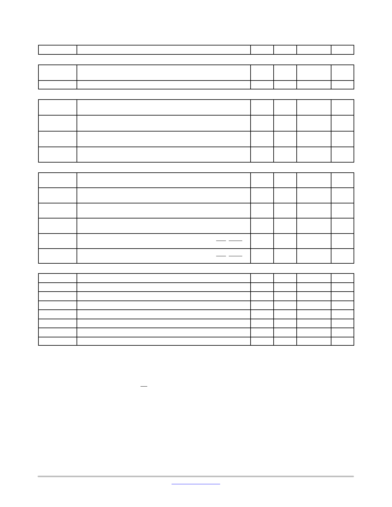
Table 5. DC CHARACTERISTICS VDD = 2.5 V ±5% or 3.3 V ±10%, GND = 0 V, TA = −40°C to +85°C (Note 5)
Symbol
Characteristic
Min Typ
Max
Unit
POWER SUPPLY
VDD Power Supply Voltage
VDD = 3.3 V
VDD = 2.5 V
2.97
2.375
3.3
2.5
3.63
2.625
V
IDD Power Supply Current
LVCMOS/LVTTL INPUTS (CLK_EN, CLK_SEL, OE)
50 mA
VIH Input HIGH Voltage
VDD = 3.3 V
VDD = 2.5 V
2
1.7
VDD + 0.3
V
VIL Input LOW Voltage
VDD = 3.3 V
VDD = 2.5 V
0.8 V
0.7
IIH Input High Current (VDD = VIN = 3.63 V)
CLK_EN, OE
CLK_SEL
5 mA
150
IIL Input LOW Current (VDD = 3.63 V, VIN = 0 V)
CLK_EN, OE
CLK_SEL
−150
−5
mA
DIFFERENTIAL INPUTS (see Figures 5 and 6) (Note 8)
VIHD
VILD
VID
Differential Input HIGH Voltage
Differential Input LOW Voltage
Differential Input Voltage (VIHD − VILD)
CLK
PCLK
CLK
PCLK
CLK
PCLK
0.5
1.5
0
0.5
0.15
0.30
VDD−0.85
VDD
VIHD−0.15
VIHD
1.3
1.0
V
V
V
VIHCMR
IIH
Common Mode Input Voltage; (Note 9)
CLK
PCLK
Input HIGH Current
VDD
=
VIN
=
3.63
V
CLK,
CLK,
PCLK
PCLK
0.5
1.5
VDD–0.85
VDD
150
5
V
mA
IIL Input LOW Current
VDD = 3.63 V, VIN = 0 V CLK, PCLK
CLK, PCLK
−5
−150
mA
LVDS OUTPUTS
VOD Differential Output Voltage
200 300 360 mV
DVOD
VOD Magnitude Change
0 40 mV
VOS Differential Output Voltage Offset Voltage
1.125 1.25
1.375
V
DVOS
VOS Magnitude Change
5 25 mV
IOZ Output High Impedance Leakage Current
−10 +10 mA
IOS Output Short Circuit Current
−5 mA
VOH Output HIGH Voltage
1.34 1.6
V
VOL Output LOW Voltage
0.9 1.06
V
Product parametric performance is indicated in the Electrical Characteristics for the listed test conditions, unless otherwise noted. Product
performance may not be indicated by the Electrical Characteristics if operated under different conditions.
NOTE: Device will meet the specifications after thermal equilibrium has been established when mounted in a test socket or printed circuit
board with maintained transverse airflow greater than 500 lfpm. Electrical parameters are guaranteed only over the declared
operating temperature range. Functional operation of the device exceeding these conditions is not implied. Device specification limit
values are applied individually under normal operating conditions and not valid simultaneously.
5. Outputs terminated 100 W across Qx and Qx, see Figure 4. DC Measurements per Figure 10 reference.
6. Vth, VIH, VIL, and VISE parameters must be complied with simultaneously.
7. Vth is applied to the complementary input when operating in single−ended mode.
8. VIHD, VILD, VID and VCMR parameters must be complied with simultaneously.
9. The common mode voltage is defined as VIH.
www.onsemi.com
5
5 Page 
NB3L8543S
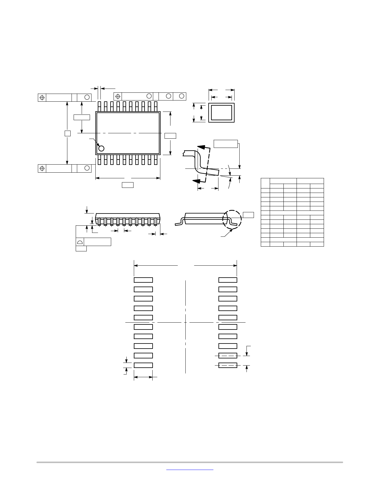
PACKAGE DIMENSIONS
TSSOP−20
CASE 948E−02
ISSUE C
0.15 (0.006) T U S
2X L/2 20
L
PIN 1
IDENT
1
0.15 (0.006) T U S
C
D
0.100 (0.004)
−T− SEATING
PLANE
20X K REF
0.10 (0.004) M T U S V S
11
B
−U−
10
A
−V−
GH
J JÍÍÍ1 ÍÍÍKÍÍÍK1 ÍÍÍ
SECTION N−N
N 0.25 (0.010)
M
N
F
DETAIL E
DETAIL E
NOTES:
1. DIMENSIONING AND TOLERANCING PER
ANSI Y14.5M, 1982.
2. CONTROLLING DIMENSION: MILLIMETER.
3. DIMENSION A DOES NOT INCLUDE MOLD
FLASH, PROTRUSIONS OR GATE BURRS.
MOLD FLASH OR GATE BURRS SHALL NOT
EXCEED 0.15 (0.006) PER SIDE.
4. DIMENSION B DOES NOT INCLUDE
INTERLEAD FLASH OR PROTRUSION.
INTERLEAD FLASH OR PROTRUSION
SHALL NOT EXCEED 0.25 (0.010) PER SIDE.
5. DIMENSION K DOES NOT INCLUDE
DAMBAR PROTRUSION. ALLOWABLE
DAMBAR PROTRUSION SHALL BE 0.08
(0.003) TOTAL IN EXCESS OF THE K
DIMENSION AT MAXIMUM MATERIAL
CONDITION.
6. TERMINAL NUMBERS ARE SHOWN FOR
REFERENCE ONLY.
7. DIMENSION A AND B ARE TO BE
DETERMINED AT DATUM PLANE −W−.
−W−
MILLIMETERS
INCHES
DIM MIN MAX MIN MAX
A 6.40 6.60 0.252 0.260
B 4.30 4.50 0.169 0.177
C --- 1.20 --- 0.047
D 0.05 0.15 0.002 0.006
F 0.50 0.75 0.020 0.030
G 0.65 BSC
0.026 BSC
H 0.27 0.37 0.011 0.015
J 0.09 0.20 0.004 0.008
J1 0.09 0.16 0.004 0.006
K 0.19 0.30 0.007 0.012
K1 0.19 0.25 0.007 0.010
L 6.40 BSC
0.252 BSC
M 0_ 8_ 0_ 8_
SOLDERING FOOTPRINT*
7.06
1
0.65
PITCH
16X
0.36
16X
1.26
DIMENSIONS: MILLIMETERS
*For additional information on our Pb−Free strategy and soldering
details, please download the ON Semiconductor Soldering and
Mounting Techniques Reference Manual, SOLDERRM/D.
www.onsemi.com
11
11 Page | ||
| Páginas | Total 12 Páginas | |
| PDF Descargar | [ Datasheet NB3L8543S.PDF ] | |
Hoja de datos destacado
| Número de pieza | Descripción | Fabricantes |
| NB3L8543S | 2.5V/3.3V Differential 2:1 MUX to 4 LVDS Clock Fanout Buffer Outputs | ON Semiconductor |
| Número de pieza | Descripción | Fabricantes |
| SLA6805M | High Voltage 3 phase Motor Driver IC. |
Sanken |
| SDC1742 | 12- and 14-Bit Hybrid Synchro / Resolver-to-Digital Converters. |
Analog Devices |
|
DataSheet.es es una pagina web que funciona como un repositorio de manuales o hoja de datos de muchos de los productos más populares, |
| DataSheet.es | 2020 | Privacy Policy | Contacto | Buscar |
