|
|
|
PDF NB100LVEP91 Data sheet ( Hoja de datos )
| Número de pieza | NB100LVEP91 | |
| Descripción | 2.5 V/3.3 V Any Level Positive Input to -2.5 V/-3.3 V LVNECL Output Translator | |
| Fabricantes | ON Semiconductor | |
| Logotipo | ||
Hay una vista previa y un enlace de descarga de NB100LVEP91 (archivo pdf) en la parte inferior de esta página. Total 11 Páginas | ||
|
No Preview Available !
NB100LVEP91
2.5 V/3.3 V Any Level
Positive Input to
-2.5 V/-3.3 V LVNECL
Output Translator
Description
The NB100LVEP91 is a triple any level positive input to NECL
output translator. The device accepts LVPECL, LVTTL, LVCMOS,
HSTL, CML or LVDS signals, and translates them to differential
LVNECL output signals (−2.5 V / −3.3 V).
To accomplish the level translation the LVEP91 requires three
power rails. The VCC pins should be connected to the positive power
supply, and the VEE pin should be connected to the negative power
supply. The GND pins are connected to the system ground plane. Both
VEE and VCC should be bypassed to ground via 0.01 mF capacitors.
Under open input conditions, the D input will be biased at VCC/2
and the D input will be pulled to GND. These conditions will force the
Q outputs to a low state, and Q outputs to a high state, which will
ensure stability.
The VBB pin, an internally generated voltage supply, is available to
this device only. For single-ended input conditions, the unused
differential input is connected to VBB as a switching reference voltage.
VBB may also rebias AC coupled inputs. When used, decouple VBB
and VCC via a 0.01 mF capacitor and limit current sourcing or sinking
to 0.5 mA. When not used, VBB should be left open.
Features
• Maximum Input Clock Frequency > 2.0 GHz Typical
• Maximum Input Data Rate > 2.0 Gb/s Typical
• 500 ps Typical Propagation Delay
• Operating Range:
♦ VCC = 2.375 V to 3.8 V; VEE = −2.375 V to −3.8 V; GND = 0 V
• Q Output will Default LOW with Inputs Open or at GND
• These Devices are Pb-Free, Halogen Free and are RoHS Compliant
www.onsemi.com
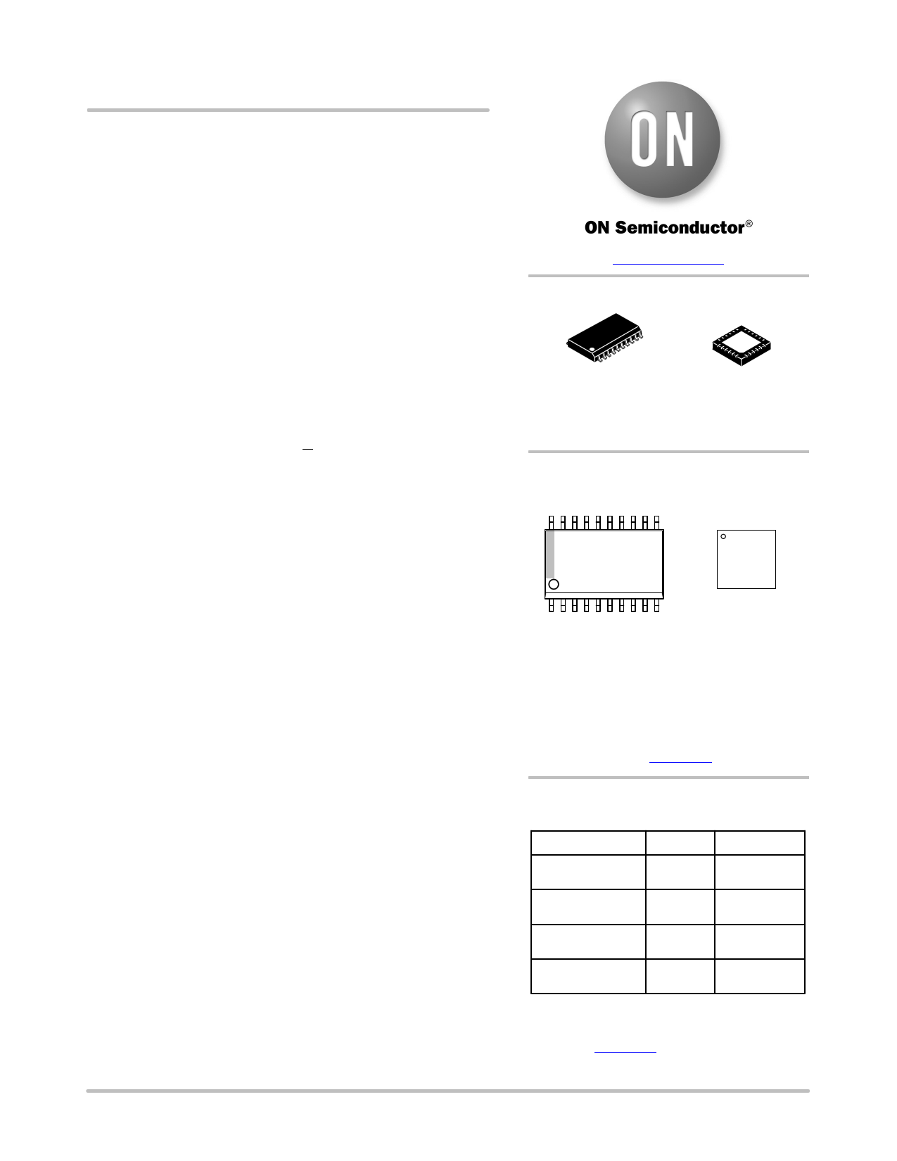
20
1
SOIC−20 WB
DW SUFFIX
CASE 751D−05
24 1
QFN−24
MN SUFFIX
CASE 485L−01
MARKING DIAGRAMS*
20
NB100LVEP91
AWLYYWWG
1
24
1 N100
VP91
ALYWG
G
A = Assembly Location
WL, L = Wafer Lot
YY, Y = Year
WW, W = Work Week
G or G = Pb-Free Package
(Note: Microdot may be in either location)
*For additional marking information, refer to
Application Note AND8002/D.
ORDERING INFORMATION
Device
Package
Shipping†
MB100LVEP91DWG
SOIC−20 WB 38 Units/Tube
(Pb-Free)
MB100LVEP91DWR2G SOIC−20 WB 1000/Tape & Reel
(Pb-Free)
MB100LVEP91MNG
QFN−24
(Pb-Free)
92 Units/Tube
MB100LVEP91MNR2G
QFN−24 3000/Tape & Reel
(Pb-Free)
†For information on tape and reel specifications, in-
cluding part orientation and tape sizes, please refer
to our Tape and Reel Packaging Specifications
Brochure, BRD8011/D.
© Semiconductor Components Industries, LLC, 2016
August, 2016 − Rev. 19
1
Publication Order Number:
NB100LVEP91/D
1 page 
NB100LVEP91
Table 5. DC CHARACTERISTICS POSITIVE INPUT (VCC = 3.3 V; VEE = −2.375 V to −3.8 V; GND = 0 V (Note 1))
−40°C
25°C
85°C
Symbol
Characteristic
Min Typ Max Min Typ Max Min Typ
ICC
VIH
VIL
VBB
VIHCMR
Positive Power Supply Current
Input HIGH Voltage (Single-Ended)
Input LOW Voltage (Single-Ended)
PECL Output Voltage Reference
Input HIGH Voltage Common Mode Range
(Differential Configuration) (Note 2)
10
2135
GND
1775
0
16 24
VCC
1675
1875 1975
3.3
10
2135
GND
1775
0
16
1875
24
VCC
1675
1975
3.3
10
2135
GND
1775
0
16
1875
IIH Input HIGH Current (@ VIH)
IIL Input LOW Current (@ VIL)
D
D
0.5
−150
150
0.5
−150
150
0.5
−150
Max
24
VCC
1675
1975
3.3
150
Unit
mA
mV
mV
mV
V
mA
mA
NOTE: Device will meet the specifications after thermal equilibrium has been established when mounted in a test socket or printed circuit
board with maintained transverse airflow greater than 500 lfpm. Electrical parameters are guaranteed only over the declared
operating temperature range. Functional operation of the device exceeding these conditions is not implied. Device specification limit
values are applied individually under normal operating conditions and not valid simultaneously.
1. Input parameters vary 1:1 with VCC. VCC can vary +0.5 / −0.925 V.
2. VIHCMR min varies 1:1 with GND. VIHCMR max varies 1:1 with VCC.
Table 6. DC CHARACTERISTICS NECL OUTPUT (VCC = 2.375 V to 3.8 V; VEE = −2.375 V to −3.8 V; GND = 0 V (Note 1))
−40°C
25°C
85°C
Symbol
Characteristic
Min Typ Max Min Typ Max Min Typ Max Unit
IEE Negative Power Supply Current
VOH Output HIGH Voltage (Note 2)
VOL Output LOW Voltage (Note 2)
40
−1145
−1945
50
−1020
−1770
60
−895
−1600
38
−1145
−1945
50
−1020
−1770
68
−895
−1600
38
−1145
−1945
50
−1020
−1770
68
−895
−1600
mA
mV
mV
NOTE: Device will meet the specifications after thermal equilibrium has been established when mounted in a test socket or printed circuit
board with maintained transverse airflow greater than 500 lfpm. Electrical parameters are guaranteed only over the declared
operating temperature range. Functional operation of the device exceeding these conditions is not implied. Device specification limit
values are applied individually under normal operating conditions and not valid simultaneously.
1. Output parameters vary 1:1 with GND.
2. All loading with 50 W resistor to GND − 2.0 V.
www.onsemi.com
5
5 Page 
NB100LVEP91
PACKAGE DIMENSIONS
QFN−24, 4x4, 0.5P
CASE 485L
ISSUE B
D
PIN 1
REFEENCE
ÉÉÉÉÉÉÉÉÉ2X
0.15 C
A
B
E
2X 0.15 C TOP VIEW
0.10 C
DETAIL B
0.08 C
NOTE 4
A3
SIDE VIEW A1
LL
L1
DETAIL A
ALTERNATE
CONSTRUCTIONS
ÉÉÇÉÉÇÉÉÇ ÉÉÇÉÉÇEXPOSEDCu
MOLD CMPD
A3
A1
A
DETAIL B
ALTERNATE TERMINAL
CONSTRUCTIONS
C
SEATING
PLANE
NOTES:
1. DIMENSIONING AND TOLERANCING PER ASME
Y14.5M, 1994.
2. CONTROLLING DIMENSION: MILLIMETERS.
3. DIMENSION b APPLIES TO PLATED TERMINAL
AND IS MEASURED BETWEEN 0.25 AND 0.30 MM
FROM THE TERMINAL TIP.
4. COPLANARITY APPLIES TO THE EXPOSED PAD
AS WELL AS THE TERMINALS.
MILLIMETERS
DIM MIN MAX
A 0.80 1.00
A1 0.00 0.05
A3 0.20 REF
b 0.20 0.30
D 4.00 BSC
D2 2.70 2.90
E 4.00 BSC
E2 2.70 2.90
e 0.50 BSC
L 0.30 0.50
L1 0.05 0.15
DETAIL A
D2
7
24X L
13
RECOMMENDED
SOLDERING FOOTPRINT
4.30
2.90
24X
0.55
E2
1
1
24
e
e/2
19
BOTTOM VIEW
24X b
0.10
0.05
CAB
C NOTE 3
2.90
4.30
0.50
PITCH
24X
0.32
DIMENSIONS: MILLIMETERS
*For additional information on our Pb-Free strategy and sol-
dering details, please download the ON Semiconductor
Soldering and Mounting Techniques Reference Manual,
SOLDERRM/D.
ECLinPS is a registered trademark of Semiconductor Components Industries, LLC (SCILLC) or its subsidiaries in the United States and/or other countries.
ON Semiconductor and are trademarks of Semiconductor Components Industries, LLC dba ON Semiconductor or its subsidiaries in the United States and/or other countries.
ON Semiconductor owns the rights to a number of patents, trademarks, copyrights, trade secrets, and other intellectual property. A listing of ON Semiconductor’s product/patent
coverage may be accessed at www.onsemi.com/site/pdf/Patent-Marking.pdf. ON Semiconductor reserves the right to make changes without further notice to any products herein.
ON Semiconductor makes no warranty, representation or guarantee regarding the suitability of its products for any particular purpose, nor does ON Semiconductor assume any liability
arising out of the application or use of any product or circuit, and specifically disclaims any and all liability, including without limitation special, consequential or incidental damages.
Buyer is responsible for its products and applications using ON Semiconductor products, including compliance with all laws, regulations and safety requirements or standards,
regardless of any support or applications information provided by ON Semiconductor. “Typical” parameters which may be provided in ON Semiconductor data sheets and/or
specifications can and do vary in different applications and actual performance may vary over time. All operating parameters, including “Typicals” must be validated for each customer
application by customer’s technical experts. ON Semiconductor does not convey any license under its patent rights nor the rights of others. ON Semiconductor products are not
designed, intended, or authorized for use as a critical component in life support systems or any FDA Class 3 medical devices or medical devices with a same or similar classification
in a foreign jurisdiction or any devices intended for implantation in the human body. Should Buyer purchase or use ON Semiconductor products for any such unintended or unauthorized
application, Buyer shall indemnify and hold ON Semiconductor and its officers, employees, subsidiaries, affiliates, and distributors harmless against all claims, costs, damages, and
expenses, and reasonable attorney fees arising out of, directly or indirectly, any claim of personal injury or death associated with such unintended or unauthorized use, even if such
claim alleges that ON Semiconductor was negligent regarding the design or manufacture of the part. ON Semiconductor is an Equal Opportunity/Affirmative Action Employer. This
literature is subject to all applicable copyright laws and is not for resale in any manner.
PUBLICATION ORDERING INFORMATION
LITERATURE FULFILLMENT:
Literature Distribution Center for ON Semiconductor
19521 E. 32nd Pkwy, Aurora, Colorado 80011 USA
Phone: 303−675−2175 or 800−344−3860 Toll Free USA/Canada
Fax: 303−675−2176 or 800−344−3867 Toll Free USA/Canada
Email: [email protected]
N. American Technical Support: 800−282−9855 Toll Free
USA/Canada
Europe, Middle East and Africa Technical Support:
Phone: 421 33 790 2910
Japan Customer Focus Center
Phone: 81−3−5817−1050
www.onsemi.com
11
ON Semiconductor Website: www.onsemi.com
Order Literature: http://www.onsemi.com/orderlit
For additional information, please contact your local
Sales Representative
NB100LVEP91/D
11 Page | ||
| Páginas | Total 11 Páginas | |
| PDF Descargar | [ Datasheet NB100LVEP91.PDF ] | |
Hoja de datos destacado
| Número de pieza | Descripción | Fabricantes |
| NB100LVEP91 | 2.5 V/3.3 V Any Level Positive Input to -2.5 V/-3.3 V LVNECL Output Translator | ON Semiconductor |
| Número de pieza | Descripción | Fabricantes |
| SLA6805M | High Voltage 3 phase Motor Driver IC. |
Sanken |
| SDC1742 | 12- and 14-Bit Hybrid Synchro / Resolver-to-Digital Converters. |
Analog Devices |
|
DataSheet.es es una pagina web que funciona como un repositorio de manuales o hoja de datos de muchos de los productos más populares, |
| DataSheet.es | 2020 | Privacy Policy | Contacto | Buscar |