|
|
|
PDF 8SLVP2106 Data sheet ( Hoja de datos )
| Número de pieza | 8SLVP2106 | |
| Descripción | LVPECL Output Fanout Buffer | |
| Fabricantes | IDT | |
| Logotipo | ||
Hay una vista previa y un enlace de descarga de 8SLVP2106 (archivo pdf) en la parte inferior de esta página. Total 24 Páginas | ||
|
No Preview Available !
Low Phase Noise, Dual 1-to-6, 3.3V, 2.5V
LVPECL Output Fanout Buffer
8SLVP2106
DATA SHEET
General Description
The 8SLVP2106 is a high-performance differential dual 1:6 LVPECL
fanout buffer. The device is designed for the fanout of high-frequency,
very low additive phase-noise clock and data signals. The
8SLVP2106 is characterized to operate from a 3.3V or 2.5V power
supply. Guaranteed output-to-output and part-to-part skew
characteristics make the 8SLVP2106 ideal for those clock distribution
applications demanding well-defined performance and repeatability.
Two independent buffers with six low skew outputs each are
available. The integrated bias voltage references enable easy
interfacing of single-ended signals to the device inputs. The device is
optimized for low power consumption and low additive phase noise.
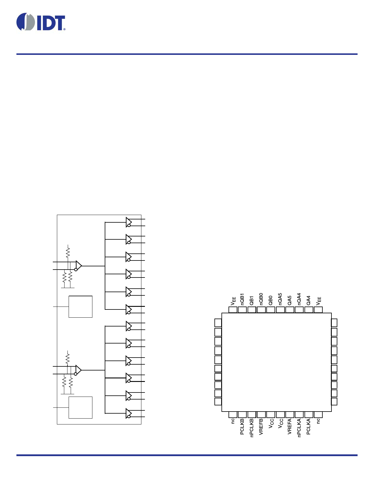
Block Diagram
PCLKA
nPCLKA
VCC
VREFA
Voltage
Reference
PCLKB
nPCLKB
VCC
VREFB
Voltage
Reference
QA0
nQA0
QA1
nQA1
QA2
nQA2
QA3
nQA3
QA4
nQA4
QA5
nQA5
QB0
nQB0
QB1
nQB1
QB2
nQB2
QB3
nQB3
QB4
nQB4
QB5
nQB5
Features
• Two 1:6, low skew, low additive jitter LVPECL fanout buffers
• Two differential clock inputs
• Differential PCLKA, nPCLKA and PCLKB, nPCLKB pairs can
accept the following differential input levels: LVDS, LVPECL, CML
• Differential PCLKA, nPCLKA and PCLKB, nPCLKB pairs can also
accept single-ended LVCMOS levels. See Applications section
Wiring the Differential Input Levels to Accept Single-ended Levels
(Figure 1A and Figure 1B).
• Maximum input clock frequency: 2GHz
• Output bank skew: 15ps (typical)
• Propagation delay: 340ps (maximum)
• Low additive phase jitter, RMS: 54fs (maximum)
fREF = 156.25MHz, VPP = 1V, 12kHz - 20MHz: VCC = 3.3V)
• Full 3.3V and 2.5V supply voltage modes
• Maximum device current consumption (IEE): 114mA
• Available in Lead-free (RoHS 6), 40-Lead VFQFN package
• -40°C to 85°C ambient operating temperature
• Supports case temperature 105°C operations
Pin Assignment
30 29 28 27 26 25 24 23 22 21
VCC 31
QB2 32
nQB2 33
QB3 34
nQB3 35
QB4 36
nQB4 37
QB5 38
nQB5 39
VCC 40
8SLVP2106i
40-lead VFQFN
6mm x 6mm x 0.925mm package body
NL Package
Top View
1 2 3 4 5 6 7 8 9 10
20 VCC
19 nQA3
18 QA3
17 nQA2
16 QA2
15 nQA1
14 QA1
13 nQA0
12 QA0
11 VCC
8SLVP2106 REVISION B 6/9/15
1 ©2015 Integrated Device Technology, Inc.
1 page 
8SLVP2106 DATA SHEET
AC Electrical Characteristics
Table 4A. AC Electrical Characteristics, VCC = 3.3V ± 5% or 2.5V ± 5%, VEE = 0V, TA = -40°C to 85°C
Symbol Parameter
Test Conditions
Minimum Typical
fREF
V/t
Input Frequency
Input Edge Rate
PCLKA, nPCLKA and PCLKB, nPCLKB
PCLKA, nPCLKA and PCLKB, nPCLKB
1.5
tPD
tsk(o)
Propagation Delay; NOTE 1
Output Skew; NOTE 2, 3
PCLKA, nPCLKA to any QAx, nQAx or
PCLKB, nPCLKB to any QBx, nQBx
for VPP = 0.1V or 0.3V
130
235
26
tsk(b)
Output Bank Skew; NOTE 3,
4
15
tsk(p)
tsk(pp)
Pulse Skew
Part-to-Part Skew; NOTE 3, 5
fREF = 100MHz
6
66
tJIT, SP
Spurious Suppression,
Coupling from QA5 to QB0
tR / tF
Output Rise/ Fall Time;
NOTE 6
fQB0 = 500MHz, VPP(PCLKB) = 0.15V,
VCMR(PCLKB) = 1V;
fQA5 = 62.5MHz, VPP(PCLKA) = 1V,
VCMR(PCLKA) = 1V
fQB0 = 500MHz, VPP(PCLKB) = 0.15V,
VCMR(PCLKB) = 1V;
fQA5 = 15.625MHz, VPP(PCLKA) = 1V,
VCMR(PCLKA) = 1V
20% to 80%
-52
-63
60 100
VPP
VCMR
Differential Input Voltage;
NOTE 7, 8
Common Mode Input
Voltage; NOTE 7, 8, 9
fREF 1.5GHz
fREF 1.5GHz
0.1
0.2
1.0
VO(pp)
Output Voltage Swing,
Peak-to-Peak
VDIFF_OU Differential Output Voltage
T Swing, Peak-to-Peak
fREF 2GHz, VCC = 2.5V ± 5%
fREF 2GHz, VCC = 3.3V ± 5%
fREF 2GHz, VCC = 2.5V ± 5%
fREF 2GHz, VCC = 3.3V ± 5%
0.31 0.46
0.33 0.49
0.62 0.92
0.66 0.98
Maximum
2
340
60
42
26
144
170
1.5
1.5
VCC – 0.3
0.62
0.66
1.24
1.32
Units
GHz
V/ns
ps
ps
ps
ps
ps
dB
dB
ps
V
V
V
V
V
V
V
NOTE: Electrical parameters are guaranteed over the specified ambient operating temperature range, which is established when the device is
mounted in a test socket with maintained transverse airflow greater than 500 lfpm. The device will meet specifications after thermal equilibrium
has been reached under these conditions.
NOTE 1: Measured from the differential input crosspoint to the differential output crosspoint.
NOTE 2: Defined as skew between outputs at the same supply voltage and with equal load conditions. Measured at the differential crosspoints.
NOTE 3: This parameter is defined in accordance with JEDEC Standard 65.
NOTE 4: Defined as skew within a bank of outputs at the same supply voltage and with equal load conditions. Measured at the differential
crosspoints.
NOTE 5: Defined as skew between outputs on different devices operating at the same supply voltage, same frequency, same temperature and
with equal load conditions. Using the same type of inputs on each device, the outputs are measured at the differential crosspoints.
NOTE 6: Characterized with input signal meeting the input edge rate minimum specification.
NOTE 7: For single-ended LVCMOS input applications, please refer to the Applications Information, Wiring the Differential Input to Accept
Single-ended Levels, Figures 1A and 1B.
NOTE 8: VIL should not be less than -0.3V. VIH should not be higher than VCC.
NOTE 9: Common mode input voltage is defined at the crosspoint.
REVISION B 6/9/15
5 LOW PHASE NOISE, DUAL 1-TO-6, 3.3V, 2.5V LVPECL OUTPUT
FANOUT BUFFER
5 Page 
8SLVP2106 DATA SHEET
3.3V LVPECL Clock Input Interface
The PCLK /nPCLK accepts LVPECL, LVDS and other differential
signals. Both differential signals must meet the VPP and VCMR input
requirements. Figures 2A to 2C show interface examples for the
PCLK/ nPCLK input driven by the most common driver types. The
input interfaces suggested here are examples only. If the driver is
from another vendor, use their termination recommendation. Please
consult with the vendor of the driver component to confirm the driver
termination requirements.
3.3V
LVPECL
Zo = 50Ω
Zo = 50Ω
3.3V
R3
125Ω
R4
125Ω
3.3V
PCLK
nPCLK
LVPECL
R1 R2
84Ω 84Ω
Input
Figure 2A. PCLK/nPCLK Input Driven by a
3.3V LVPECL Driver
Figure 2B. PCLK/nPCLK Input Driven by a
3.3V LVPECL Driver with AC Couple
3.3V
LVDS
Zo = 50
Zo = 50
3.3V
R1
100
PCLK
nPCLK
LVPECL
Input
Figure 2C. PCLK/nPCLK Input Driven by a
3.3V LVDS Driver
REVISION B 6/9/15
11 LOW PHASE NOISE, DUAL 1-TO-6, 3.3V, 2.5V LVPECL OUTPUT
FANOUT BUFFER
11 Page | ||
| Páginas | Total 24 Páginas | |
| PDF Descargar | [ Datasheet 8SLVP2106.PDF ] | |
Hoja de datos destacado
| Número de pieza | Descripción | Fabricantes |
| 8SLVP2104 | LVPECL Output Fanout Buffer | IDT |
| 8SLVP2106 | LVPECL Output Fanout Buffer | IDT |
| 8SLVP2108 | LVPECL Output Fanout Buffer | IDT |
| Número de pieza | Descripción | Fabricantes |
| SLA6805M | High Voltage 3 phase Motor Driver IC. |
Sanken |
| SDC1742 | 12- and 14-Bit Hybrid Synchro / Resolver-to-Digital Converters. |
Analog Devices |
|
DataSheet.es es una pagina web que funciona como un repositorio de manuales o hoja de datos de muchos de los productos más populares, |
| DataSheet.es | 2020 | Privacy Policy | Contacto | Buscar |