|
|
PDF 9DBV0631 Data sheet ( Hoja de datos )
| Número de pieza | 9DBV0631 | |
| Descripción | 6-output 1.8V PCIe Gen1-2-3 ZDB/FOB | |
| Fabricantes | IDT | |
| Logotipo |  |
|
Hay una vista previa y un enlace de descarga de 9DBV0631 (archivo pdf) en la parte inferior de esta página. Total 17 Páginas | ||
|
No Preview Available !
6-output 1.8V PCIe Gen1-2-3 ZDB/FOB
9DBV0631
DATASHEET
Description
The 9DBV0631 is a member of IDT's 1.8V Very-Low-Power
(VLP) PCIe family. The device has 6 output enables for clock
management and 3 selectable SMBus addresses.
Recommended Application
1.8V PCIe Gen1-2-3 Zero Delay/Fanout Buffer (ZDB/FOB)
Output Features
• 6 - 1-200 MHz Low-Power (LP) HCSL DIF pairs
Key Specifications
• DIF additive cycle-to-cycle jitter <5ps
• DIF output-to-output skew <60ps
• DIF additive phase jitter is <100fs rms for PCIe Gen3
• DIF additive phase jitter <300fs rms for SGMII
Block Diagram
Features/Benefits
• LP-HCSL outputs; save 12 resistors compared to standard
PCIe devices
• 55mW typical power consumption in PLL mode; minimal
power consumption
• Outputs can optionally be supplied from any voltage
between 1.05 and 1.8V; maximum power savings
• OE# pins; support DIF power management
• HCSL-compatible differential input; can be driven by
common clock sources
• Spread Spectrum tolerant; allows reduction of EMI
• Programmable Slew rate for each output; allows tuning for
various line lengths
• Programmable output amplitude; allows tuning for various
application environments
• Pin/software selectable PLL bandwidth and PLL Bypass;
minimize phase jitter for each application
• Outputs blocked until PLL is locked; clean system start-up
• Configuration can be accomplished with strapping pins;
SMBus interface not required for device control
• 3.3V tolerant SMBus interface works with legacy
controllers
• Space saving 40-pin 5x5mm MLF; minimal board space
• 3 selectable SMBus addresses; multiple devices can easily
share an SMBus segment
vOE(5:0)#
6
CLK_IN
CLK_IN#
vSADR
^vHIBW_BYPM_LOBW#
^CKPWRGD_PD#
SDATA_3.3
SCLK_3.3
SS-
Compatible
PLL
CONTROL
LOGIC
DIF5
DIF4
DIF3
DIF2
DIF1
DIF0
9DBV0631 REVISION H 07/27/16 1 ©2016 Integrated Device Technology, Inc.
1 page 
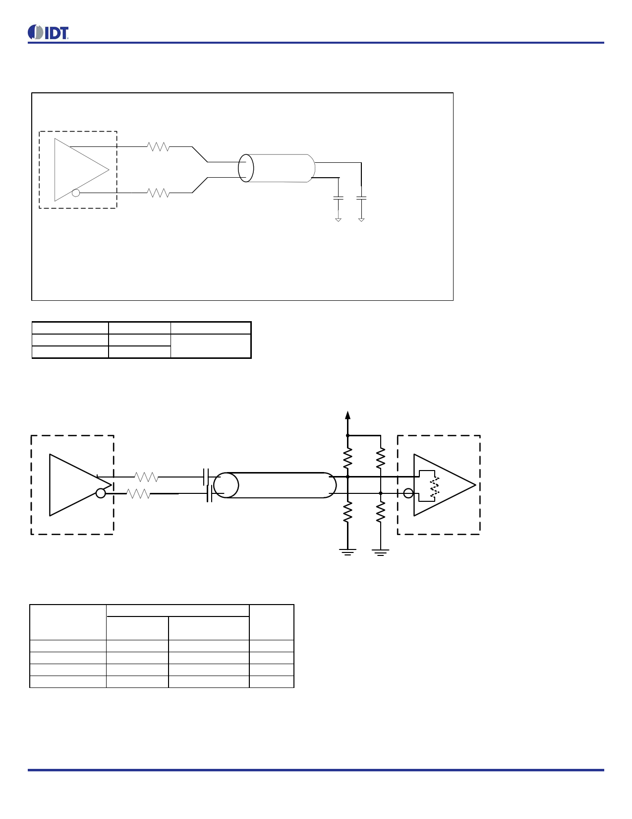
Test Loads
Low-Power Differential Output Test Load
Rs
Rs
5 inches
Zo=100W
2pF 2pF
9DBV0631 DATASHEET
Alternate Differential Output Terminations
Rs Zo Units
33 100 Ohms
27 85
Driving LVDS
Driving LVDS
Rs
Rs
Cc
Cc
L4
Driving LVDS inputs
Value
Receiver has Receiver does not
Component
termination have termination Note
R7a, R7b
10K ohm
140 ohm
R8a, R8b
5.6K ohm
75 ohm
Cc
0.1 uF
0.1 uF
Vcm
1.2 volts
1.2 volts
3.3 Volts
R7a R7b
R8a R8b
LVDS CLK
Input
REVISION H 07/27/16
5 6-OUTPUT 1.8V PCIE GEN1-2-3 ZDB/FOB
5 Page 
9DBV0631 DATASHEET
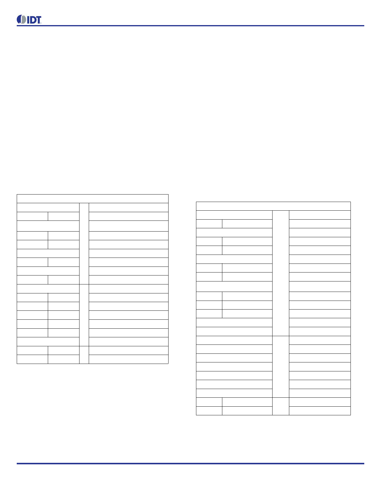
General SMBus Serial Interface Information
How to Write
• Controller (host) sends a start bit
• Controller (host) sends the write address
• IDT clock will acknowledge
• Controller (host) sends the beginning byte location = N
• IDT clock will acknowledge
• Controller (host) sends the byte count = X
• IDT clock will acknowledge
• Controller (host) starts sending Byte N through Byte
N+X-1
• IDT clock will acknowledge each byte one at a time
• Controller (host) sends a Stop bit
Index Block Write Operation
Controller (Host)
IDT (Slave/Receiver)
T starT bit
Slave Address
WR WRite
Beginning Byte = N
Data Byte Count = X
Beginning Byte N
O
O
O
Byte N + X - 1
P stoP bit
ACK
ACK
ACK
ACK
O
O
O
ACK
Note: Read/Write address is latched on SADR pin.
How to Read
• Controller (host) will send a start bit
• Controller (host) sends the write address
• IDT clock will acknowledge
• Controller (host) sends the beginning byte location = N
• IDT clock will acknowledge
• Controller (host) will send a separate start bit
• Controller (host) sends the read address
• IDT clock will acknowledge
• IDT clock will send the data byte count = X
• IDT clock sends Byte N+X-1
• IDT clock sends Byte 0 through Byte X (if X(H) was
written to Byte 8)
• Controller (host) will need to acknowledge each byte
• Controller (host) will send a not acknowledge bit
• Controller (host) will send a stop bit
Index Block Read Operation
Controller (Host)
T starT bit
Slave Address
WR WRite
Beginning Byte = N
RT Repeat starT
Slave Address
RD ReaD
IDT
ACK
ACK
ACK
ACK
ACK
O
O
O
N Not acknowledge
P stoP bit
Data Byte Count=X
Beginning Byte N
O
O
O
Byte N + X - 1
REVISION H 07/27/16
11 6-OUTPUT 1.8V PCIE GEN1-2-3 ZDB/FOB
11 Page | ||
| Páginas | Total 17 Páginas | |
| PDF Descargar | [ Datasheet 9DBV0631.PDF ] | |
Hoja de datos destacado
| Número de pieza | Descripción | Fabricantes |
| 9DBV0631 | 6-output 1.8V PCIe Gen1-2-3 ZDB/FOB | IDT |
| Número de pieza | Descripción | Fabricantes |
| SLA6805M | High Voltage 3 phase Motor Driver IC. |
Sanken |
| SDC1742 | 12- and 14-Bit Hybrid Synchro / Resolver-to-Digital Converters. |
Analog Devices |
|
DataSheet.es es una pagina web que funciona como un repositorio de manuales o hoja de datos de muchos de los productos más populares, |
| DataSheet.es | 2020 | Privacy Policy | Contacto | Buscar |
