|
|
PDF WS2596B Data sheet ( Hoja de datos )
| Número de pieza | WS2596B | |
| Descripción | High Efficiency Charger Control IC | |
| Fabricantes | Winsemi | |
| Logotipo |  |
|
Hay una vista previa y un enlace de descarga de WS2596B (archivo pdf) en la parte inferior de esta página. Total 9 Páginas | ||
|
No Preview Available !
WS2596B Product Description
WS2596B High Efficiency Charger Control IC
Features
Standby power<75mw
Low stat-up current,<1uA
High efficiency(Meet Energy Star 6.0)
Internal random Frequency jitter to Reduce System EMI
Internal leading edge blanking
Cycle by cycle current limit
VCC UVLO and Over Voltage Protection
±5% CC、CV accuracy
Good dynamic transient(10%--any load)
CS pin and CS resistor Open/Short protection
FB Upper/Lower resistor Open/Short protection
IC GND open protection
Output over voltage protection
Output under voltage protection
Over temperature protection
Intelligent temperature regulation (When the
temperature over 133℃,the output power will be
reduced.)
Secondary SBD short protection
Transformer saturation protection
CS double peak threshold,suppress audio noise
Slope drive technology,reduce driving loss
External proprietary adjustable cable voltage drop
Compensation
Internal proprietary adjustable line compensation for CC
Variation
Internal BJT
SOP-7 package
Description
WS2596B is a high performance AC/DC power supply
controller for battery charger and adapter applications.The
device uses Pulse Frequency Modulation (PFM) method to
build discontinuous conduction mode (DCM)flyback power
supplies.
WS2596B provides accurate constant voltage, constant
current (CV/CC) regulation without requiring an opto-coupler
and the secondary control circuitry. It also eliminates the need
of loop compensation circuitry while maintaining good stability.
WS2596B can achieve excellent regulation and high average
efficiency(meet Energy star 6.0), yet meets standby power
less than 75mW.
WS2596B has a proprietary cable voltage drop
compensation function. Internal random frequency
modulation to reduce system EMI.
WS2596B is available in SOP-7 package.
Typical Appliction
Adapters/Chargers for Cell/cordless Phones, PDAs,
MP3 and Other Portable Devices
LED driver
WINSEMI MICROELECTRONICS
WINSEMI MICROELECTRONICS
WINSEMI MICROELECTRONICS
Copyright@Winsemi Microelectronics Co., Ltd., All right reserved.
WINSEMI MICROELECTRONICS
WINSEMI MICROELECTRONICS
A2 0318
1 page 
WS2596B Product Description
Thermal section
Intelligent thermal control
threshold
OTP threshold
Tz
Totp
Output power start to
reduce
Restart
133
150
℃
℃
Function Description
Start-up and UVLO
At the phase of power-on, the rectified high voltage DC
charges the capacitor of VCC through the start-up resistor.
When VCC rises to 16.3V, the IC enters normal operation,
then switching begins and the output voltage begins to rise.
The VCC bypass capacitor must supply the IC until the
output voltage builds up enough to provide power from the
auxiliary winding to sustain the VCC. The under-voltage
threshold of VCC is 4.2V, the control circuit will turn off the
output, then the Vcc capacitor will be charged again.
Constant primary peak current
The primary current ip(t) is sensed by a current sense
resistor Rcs, the current rises up linearly at a rate of:
dip(t)
dt
Vg (t )
Lm
Lm is primary inductance
(1)
P
1
2
Lm
Ipk 2
f sw
(4)
Where fsw is the switching frequency. When the
peak current Ipk is constant, the output power depends on
the switching frequency fsw.
Constant Voltage Operation
The WS2596B captures the auxiliary winding feedback
voltage at FB pin and operates in constant-voltage (CV) mode
to regulate the output voltage. Assuming the secondary
winding is master, the auxiliary winding is slave during the D1
on-time. The auxiliary voltage is given by:
Vaux
Naux
Vs
Ns
And Vs Vo Vd
So
Vaux
Naux
Ns
(Vo
Vd ) ,
.
Where Vd is the diode forward drop voltage.
So the output will be constant when the VFB is constant to 4V.
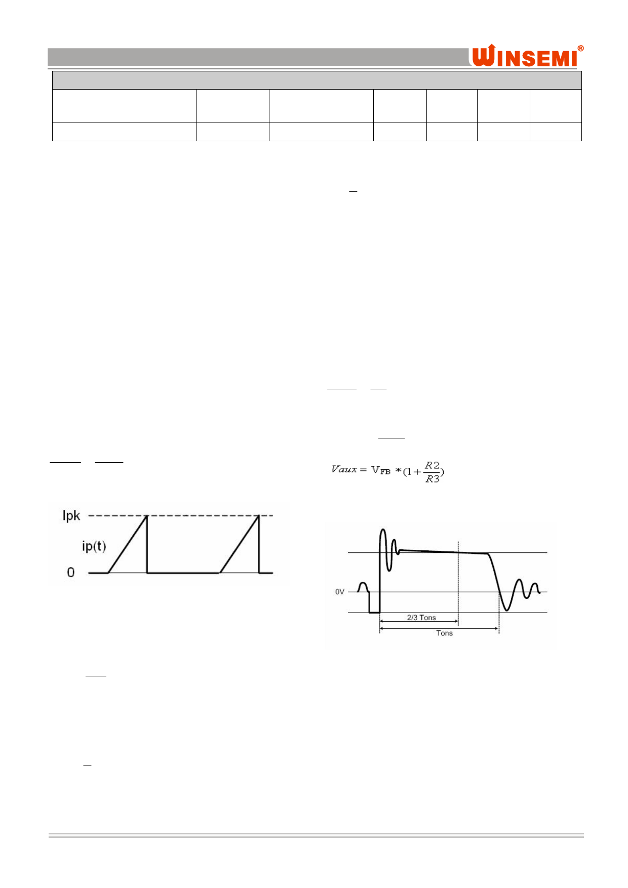
Primary current waveform
As illustrated in top figure,when the current ip(t) rises up to
Ipk, the switch turns off. The constant peak current is given
by:
Ipk
Vcs
Rcs
, Vcs is internal limited to 0.5V
(2)
The energy stored in the magnetizing inductance Lm each
cycle is :
Eg
1
2
Lm
Ipk 2
(3)
So the power transferring from the input to the output is given
by:
Auxiliary voltage waveform
The output voltage is different from the secondary voltage in a
diode forward drop voltage that depends on the current. If the
secondary voltage is always detected at a fixed secondary
current, the difference between the output voltage and the
secondary voltage will be a fixed Vd. The voltage detection
point is at two-thirds of the D1 on-time. The CV loop control
function of WS2596B then generates a D1 off-time to regulate
the output voltage.
WINSEMI MICROELECTRONICS
WINSEMI MICROELECTRONICS
WINSEMI MICROELECTRONICS
www.winsemi.com Tel : +86-755-8250 6288 Fax : +86-755-8250 6299
WINSEMI MICROELECTRONICS
WINSEMI MICROELECTRONICS
5/9
5 Page | ||
| Páginas | Total 9 Páginas | |
| PDF Descargar | [ Datasheet WS2596B.PDF ] | |
Hoja de datos destacado
| Número de pieza | Descripción | Fabricantes |
| WS2596B | High Efficiency Charger Control IC | Winsemi |
| Número de pieza | Descripción | Fabricantes |
| SLA6805M | High Voltage 3 phase Motor Driver IC. |
Sanken |
| SDC1742 | 12- and 14-Bit Hybrid Synchro / Resolver-to-Digital Converters. |
Analog Devices |
|
DataSheet.es es una pagina web que funciona como un repositorio de manuales o hoja de datos de muchos de los productos más populares, |
| DataSheet.es | 2020 | Privacy Policy | Contacto | Buscar |
