|
|
|
PDF 87972I-147 Data sheet ( Hoja de datos )
| Número de pieza | 87972I-147 | |
| Descripción | 1-to-12 LVCMOS/LVTTL Clock Multiplier/Zero Delay Buffer | |
| Fabricantes | IDT | |
| Logotipo | ||
Hay una vista previa y un enlace de descarga de 87972I-147 (archivo pdf) en la parte inferior de esta página. Total 18 Páginas | ||
|
No Preview Available !
Low Skew, 1-to-12 LVCMOS/LVTTL
Clock Multiplier/Zero Delay Buffer
87972I-147
Datasheet
General Description
The 87972I-147 is a low skew, LVCMOS/LVTTL Clock Generator
and a member of the family of High Performance Clock Solutions
from IDT. The 87972I-147 has three selectable inputs and
provides 14 LVCMOS/LVTTL outputs.
The 87972I-147 is a highly flexible device. Using the crystal
oscillator input, it can be used to generate clocks for a system. All
of these clocks can be the same frequency or the device can be
configured to generate up to three different frequencies among the
three output banks. Using one of the single ended inputs, the
87972I-147 can be used as a zero delay buffer/multiplier/ divider in
clock distribution applications.
The three output banks and feedback output each have their own
output dividers which allows the device to generate a multitude of
different bank frequency ratios and output-to-input frequency
ratios. In addition, 2 outputs in Bank C (QC2, QC3) can be select-
ed to be inverting or non-inverting. The output frequency range is
10MHz to 150MHz. Input frequency range is 6MHz to 150MHz.
The 87972I-147 also has a QSYNC output which can be used or
system synchronization purposes. It monitors Bank A and Bank C
outputs and goes low one period of the faster clock prior to
coincident rising edges of Bank A and Bank C clocks. QSYNC
then goes high again when the coincident rising edges of Bank A
and Bank C occur. This feature is used primarily in applications
where Bank A and Bank C are running at different frequencies,
and is particularly useful when they are running at non-integer
multiples of one another.
Example Applications:
1.System Clock generator: Use a 16.66 MHz Crystal to generate
eight 33.33MHz copies for PCI and four 100MHz copies for the
CPU or PCI-X.
2.Line Card Multiplier: Multiply 19.44MHz from a back plane to
77.76MHz for the line Card ASICs and Serdes.
3.Zero Delay buffer for Synchronous memory: Fan out up to
twelve 100MHz copies from a memory controller reference
clock to the memory chips on a memory module with zero delay.
Features
• Fully integrated PLL
• Fourteen LVCMOS/LVTTL outputs; (12)clocks, (1)feedback,
(1)sync
• Selectable crystal oscillator interface or LVCMOS/LVTTL
reference clock inputs
• CLK0, CLK1 can accept the following input levels:
LVCMOS or LVTTL
• Output frequency range: 10MHz to 150MHz
• VCO range: 240MHz to 500MHz
• Output skew: 200ps (maximum)
• Cycle-to-cycle jitter, (all banks ÷4): 55ps (maximum)
• Full 3.3V supply voltage
• -40°C to 85°C ambient operating temperature
• Compatible with PowerPC™and Pentium™Microprocessors
• Available in lead-free (RoHS 6)packages.
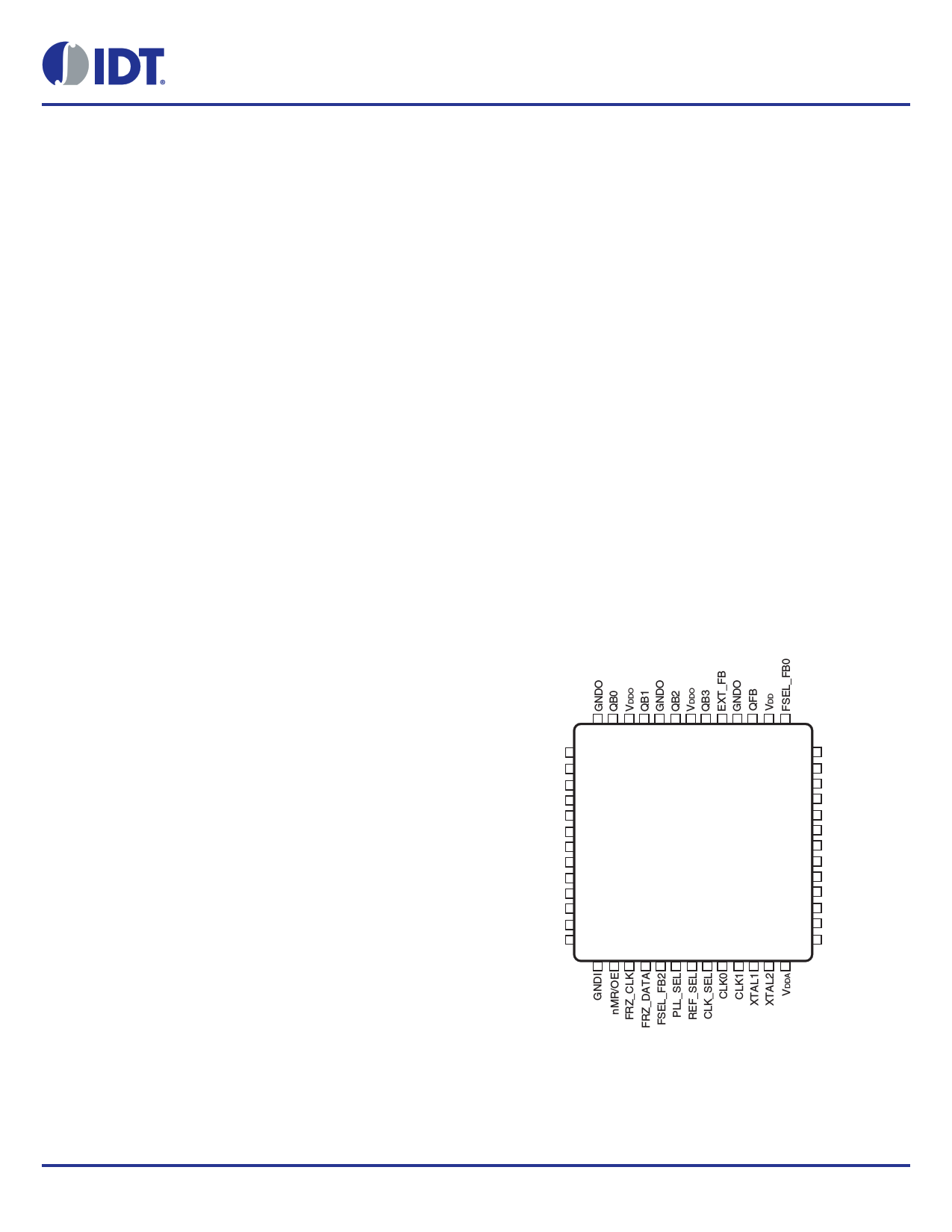
Pin Assignment
39 38 37 36 35 34 33 32 31 30 29 28 27
FSEL_B1
FSEL_B0
FSEL_A1
FSEL_A0
QA3
VDDO
QA2
GNDO
QA1
VDDO
QA0
GNDO
VCO_SEL
40
41
42
43
44
45
46
47
48
49
50
51
52
1
26
25
24
23
22
21
20
19
18
17
16
15
14
2 3 4 5 6 7 8 9 10 11 12 13
FSEL_FB1
QSYNC
GNDO
QC0
VDDO
QC1
FSEL_C0
FSEL_C1
QC2
VDDO
QC3
GNDO
INV_CLK
©2015 Integrated Device Technology, Inc
87972I-147
52-Lead LQFP
10mm x 10mm x 1.4mm package body
Y Package
Top View
1 December 7, 2015
1 page 
87972I-147 Datasheet
Table 2. Pin Characteristics
Symbol
CIN
RPULLUP
CPD
ROUT
Parameter
Input Capacitance
Input Pullup Resistor
Power Dissipation Capacitance
(per output)
Output Impedance
Test Conditions
VDD, VDDA, VDDO = 3.465V
Minimum
5
Typical
4
51
7
Maximum
18
12
Units
pF
k
pF
Function Tables
Table 3A. Output Bank Configuration Select Function Table
Inputs
Outputs
Inputs
FSEL_A1 FSEL_A0 QA FSEL_B1 FSEL_B0
0 0 ÷4 0 0
0 1 ÷6 0 1
1 0 ÷8 1 0
1 1 ÷12 1 1
Outputs
QB
÷4
÷6
÷8
÷10
Inputs
FSEL_C1 FSEL_C0
00
01
10
11
Outputs
QC
÷2
÷4
÷6
÷8
Table 3B. Feedback Configuration Select Function Table
Inputs
Outputs
FSEL_FB2 FSEL_FB1 FSEL_FB0
QFB
000
÷4
001
÷6
010
÷8
011
÷10
100
÷8
101
÷12
110
÷16
111
÷20
Table 3C. Control Input Select Function Table
Control Pin
Logic 0
Logic 1
VCO_SEL
VCO/2
VCO
REF_SEL
CLK0 or CLK1
XTAL
CLK_SEL
CLK0
CLK1
PLL_SEL
BYPASS PLL
Enable PLL
nMR/OE
Master Reset/Output Hi-Z
Enable Outputs
INV_CLK
Non-Inverted QC2, QC3
Inverted QC2, QC3
©2015 Integrated Device Technology, Inc
5
December 7, 2015
5 Page 
87972I-147 Datasheet
Crystal Input Interface
The 87972I-147 has been characterized with 18 pF parallel resonant crystals. External capacitors are not required for this crystal interface.
While layout the PC board, it is recommended to have spare footprints capacitor C1 and C2. If required, the spare C1 and C2 footprints can be
used for fine tuned further for more accurate frequency. The possible C1 and C2 value are ranged from 2pF – 25pF. The suggest footprint size
is 0402 or 0603.
X1
18pF Parallel Crystal
C1
Spare
XTAL_IN
C2
Spare
XTAL_OUT
Figure 3. Crystal Input Interface
LVCMOS to XTAL Interface
The XTAL_IN input can accept a single-ended LVCMOS signal through an AC coupling capacitor. A general interface diagram is shown in Figure
4. The XTAL_OUT pin can be left floating. The input edge rate can be as slow as 10ns. For LVCMOS inputs, it is recommended that the
amplitude be reduced from full swing to half swing in order to prevent signal interference with the power rail and to reduce noise. This
configuration requires that the output impedance of the driver (Ro) plus the series resistance (Rs) equals the transmission line impedance. In
addition, matched termination at the crystal input will attenuate the signal in half. This can be done in one of two ways. First, R1 and R2 in
parallel should equal the transmission line impedance. For most 50 applications, R1 and R2 can be 100. This can also be accomplished by
removing R1 and making R2 50.
VCC
VCC
R1
Ro Rs 50Ω
0.1µf
XTAL_IN
Zo = Ro + Rs
R2
XTAL_OUT
Figure 4. General Diagram for LVCMOS Driver to XTAL Input Interface
©2015 Integrated Device Technology, Inc
11
December 7, 2015
11 Page | ||
| Páginas | Total 18 Páginas | |
| PDF Descargar | [ Datasheet 87972I-147.PDF ] | |
Hoja de datos destacado
| Número de pieza | Descripción | Fabricantes |
| 87972I-147 | 1-to-12 LVCMOS/LVTTL Clock Multiplier/Zero Delay Buffer | IDT |
| Número de pieza | Descripción | Fabricantes |
| SLA6805M | High Voltage 3 phase Motor Driver IC. |
Sanken |
| SDC1742 | 12- and 14-Bit Hybrid Synchro / Resolver-to-Digital Converters. |
Analog Devices |
|
DataSheet.es es una pagina web que funciona como un repositorio de manuales o hoja de datos de muchos de los productos más populares, |
| DataSheet.es | 2020 | Privacy Policy | Contacto | Buscar |