|
|
|
PDF CD4016BMS Data sheet ( Hoja de datos )
| Número de pieza | CD4016BMS | |
| Descripción | CMOS Quad Bilateral Switch | |
| Fabricantes | Intersil Corporation | |
| Logotipo | ||
Hay una vista previa y un enlace de descarga de CD4016BMS (archivo pdf) en la parte inferior de esta página. Total 10 Páginas | ||
|
No Preview Available !
CD4016BMS
November 1994
CMOS Quad Bilateral Switch
Features
Applications
• Transmission or Multiplexing of Analog or Digital Signals • Analog Signal Switching/Multiplexing
• High Voltage Type (20V Rating)
• Signal Gating
• 20V Digital or ±10V Peak-to-Peak Switching
• 280Ω Typical On-State Resistance for 15V Operation
• Squelch Control
• Chopper
• Switch On-State Resistance Matched to Within 10Ω
Typ. Over 15V Signal Input Range
• High On/Off Output Voltage Ratio: 65dB Typ. at FIS =
10kHz, RL = 10kΩ
• High Degree of Linearity: <0.5% Distortion Typ. at FIS
= 1kHz, VIS = 5Vp-p, VDD-VSS ≥ 10V, RL = 10kΩ
• Extremely Low Off State Switch Leakage Resulting in
Very Low Offset Current and High Effective Off State
Resistance: 100pA Typ. at VDD-VSS = 18V, TA = 25oC
• Extremely High Control Input Impedance (Control cir-
cuit Isolated from Signal Circuit: 1012Ω Typ.
• Low Crosstalk Between Switches: -50dB Typ. at FIS =
0.9MHz, RL = 1kΩ
• Matched Control Input to Signal Output
Capacitance: Reduces Output Signal Transients
• Frequency Response, Switch On = 40MHz (Typ.)
• 100% Tested for Quiescent Current at 20V
• Maximum Control Input Current of 1µA at 18V Over Full
Package Temperature Range; 100nA at 18V at +25oC
• 5V, 10V and 15V Parametric Ratings
• Modulator
• Demodulator
• Commutating Switch
• Digital Signal Switching/Multiplexing
• CMOS Logic Implementation
• Analog to Digital & Digital to Analog Conversion
• Digital Control of Frequency, Impedance, Phase, and
Analog Signal Gain
Description
CD4016BMS Series types are quad bilateral switches intended
for the transmission or multiplexing of analog or digital signals.
Each of the four independent bilateral switches has a single con-
trol signal input which simultaneously biases both the p and n
device in a given switch on or off.
The CD4016BMS is supplied in these 14 lead outline packages:
Braze Seal DIP H4Q
Frit Seal DIP
H1B
Ceramic Flatpack H3W
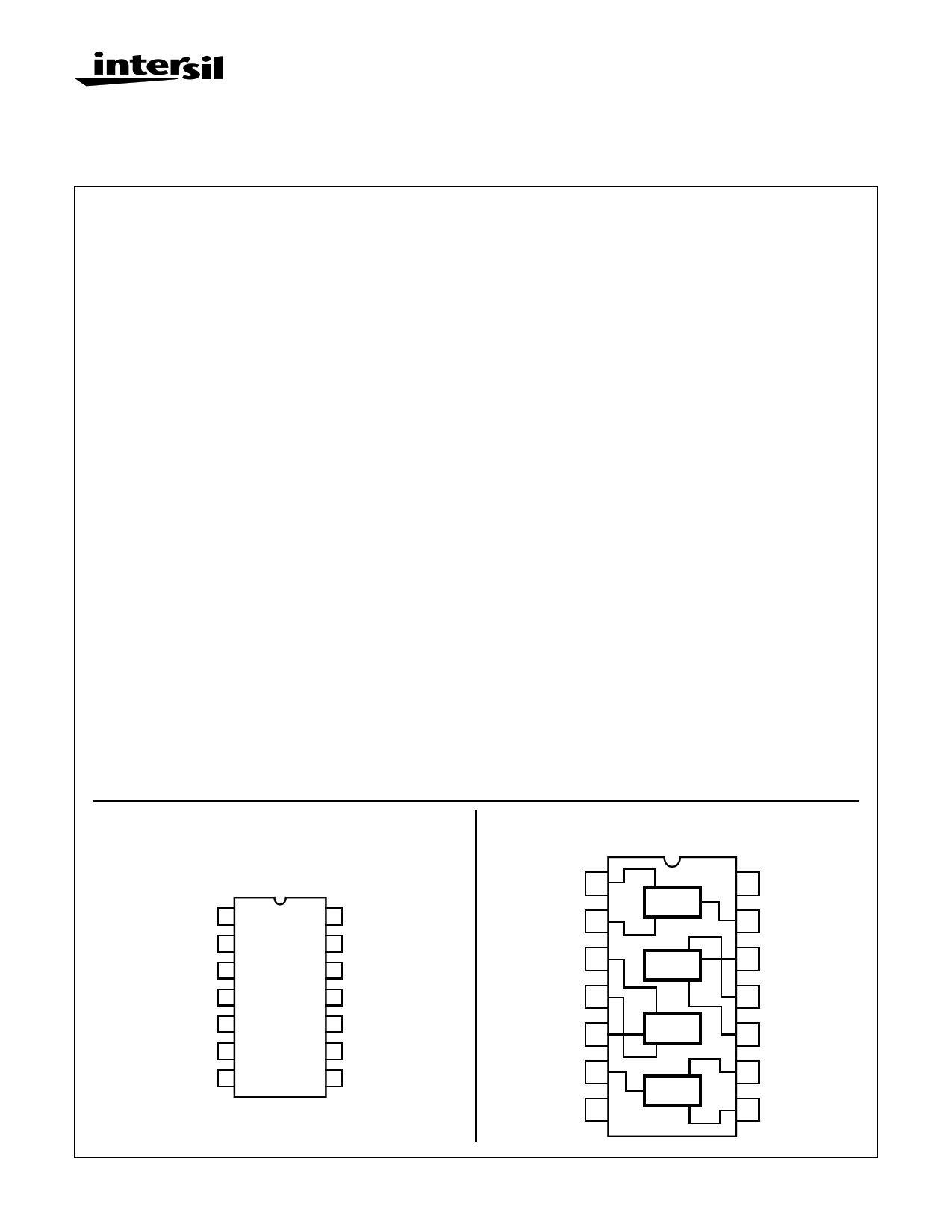
Pinout
CD4016BMS
TOP VIEW
SIG A IN 1
SIG A OUT 2
SIG B IN 3
SIG B OUT 4
CONTROL B 5
CONTROL C 6
VSS 7
14 VDD
13 CONTROL A
12 CONTROL D
11 SIG D IN
10 SIG D OUT
9 SIG C OUT
8 SIG C IN
Functional Diagram
IN/OUT
SIG A
OUT/IN
1
2
OUT/IN
SIG B
IN/OUT
3
4
CONTROL B 5
CONTROL C 6
VSS 7
SW
A
SW
D
SW
B
SW
C
14 VDD
13 CONTROL A
12 CONTROL D
11 IN/OUT
SIG D
10 OUT/IN
9 OUT/IN
SIG C
8 IN/OUT
CAUTION: These devices are sensitive to electrostatic discharge; follow proper IC Handling Procedures.
1-888-INTERSIL or 321-724-7143 | Copyright © Intersil Corporation 1999
7-733
File Number 3296
1 page 
Specifications CD4016BMS
TABLE 6. APPLICABLE SUBGROUPS (Continued)
CONFORMANCE GROUP
METHOD
GROUP A SUBGROUPS
Interim Test 3 (Post Burn-In)
100% 5004
1, 7, 9
PDA (Note 1)
100% 5004
1, 7, 9, Deltas
Final Test
100% 5004
2, 3, 8A, 8B, 10, 11
Group A
Sample 5005
1, 2, 3, 7, 8A, 8B, 9, 10, 11
Group B
Subgroup B-5
Sample 5005
1, 2, 3, 7, 8A, 8B, 9, 10, 11, Deltas
Subgroup B-6
Sample 5005
1, 7, 9
Group D
Sample 5005
1, 2, 3, 8A, 8B, 9
NOTE: 1. 5% Parameteric, 3% Functional; Cumulative for Static 1 and 2.
READ AND RECORD
IDD, IOL5, IOH5A
Subgroups 1, 2, 3, 9, 10, 11
Subgroups 1, 2 3
CONFORMANCE GROUPS
Group E Subgroup 2
TABLE 7. TOTAL DOSE IRRADIATION
TEST
METHOD
PRE-IRRAD
POST-IRRAD
5005
1, 7, 9
Table 4
READ AND RECORD
PRE-IRRAD
POST-IRRAD
1, 9 Table 4
TABLE 8. BURN-IN AND IRRADIATION TEST CONNECTIONS
OSCILLATOR
FUNCTION
Static Burn-In 1
Note 1
OPEN
2, 3, 9, 10
GROUND
1, 4-8, 11-13
VDD
14
9V ± -0.5V
50kHz
25kHz
Static Burn-In 2
Note 1
2, 3, 9, 10
7 1, 4-6, 8, 11-14
Dynamic Burn-
In Note 1
-
7
14
2, 3, 9, 10
5, 6, 12, 13
1, 4, 8, 11
Irradiation
Note 2
2, 3, 9, 10
7 1, 4-6, 8, 11-14
NOTE:
1. Each pin except VDD and GND will have a series resistor of 10K ± 5%, VDD = 18V ± 0.5V
2. Each pin except VDD and GND will have a series resistor of 47K ± 5%; Group E, Subgroup 2, sample size is 4 dice/wafer, 0 failures,
VDD = 10V ± 0.5V
Schematic Diagram
VDD
CONTROL
VC
IN/OUT
VSS
n
p
OUT/IN
FIGURE 1. 1 OF 4 IDENTICAL SECTIONS
All Intersil semiconductor products are manufactured, assembled and tested under ISO9000 quality systems certification.
Intersil products are sold by description only. Intersil Corporation reserves the right to make changes in circuit design and/or specifications at any time without
notice. Accordingly, the reader is cautioned to verify that data sheets are current before placing orders. Information furnished by Intersil is believed to be accurate
and reliable. However, no responsibility is assumed by Intersil or its subsidiaries for its use; nor for any infringements of patents or other rights of third parties which
may result from its use. No license is granted by implication or otherwise under any patent or patent rights of Intersil or its subsidiaries.
For information regarding Intersil Corporation and its products, see web site http://www.intersil.com
737
5 Page | ||
| Páginas | Total 10 Páginas | |
| PDF Descargar | [ Datasheet CD4016BMS.PDF ] | |
Hoja de datos destacado
| Número de pieza | Descripción | Fabricantes |
| CD4016BM | Quad Bilateral Switch | National Semiconductor |
| CD4016BMS | CMOS Quad Bilateral Switch | Intersil Corporation |
| Número de pieza | Descripción | Fabricantes |
| SLA6805M | High Voltage 3 phase Motor Driver IC. |
Sanken |
| SDC1742 | 12- and 14-Bit Hybrid Synchro / Resolver-to-Digital Converters. |
Analog Devices |
|
DataSheet.es es una pagina web que funciona como un repositorio de manuales o hoja de datos de muchos de los productos más populares, |
| DataSheet.es | 2020 | Privacy Policy | Contacto | Buscar |