|
|
|
PDF AD7988-5 Data sheet ( Hoja de datos )
| Número de pieza | AD7988-5 | |
| Descripción | 16-Bit Lower Power PulSAR ADCs | |
| Fabricantes | Analog Devices | |
| Logotipo | ||
Hay una vista previa y un enlace de descarga de AD7988-5 (archivo pdf) en la parte inferior de esta página. Total 23 Páginas | ||
|
No Preview Available !
Data Sheet
16-Bit Lower Power
PulSAR ADCs in MSOP/LFCSP
AD7988-1/AD7988-5
FEATURES
Low power dissipation
AD7988-1
400 µW at 100 kSPS (VDD only)
700 µW at 100 kSPS (total)
AD7988-5
2 mW at 500 kSPS (VDD only)
3.5 mW at 500 kSPS (total)
16-bit resolution with no missing codes
Throughput: 100 kSPS/500 kSPS options
INL: ±0.6 LSB typical, ±1.25 LSB maximum
SINAD: 91.5 dB at 10 kHz
THD: −114 dB at 10 kHz
Pseudo differential analog input range
0 V to VREF with VREF from 2.5 V to 5.5 V
No pipeline delay
Single-supply 2.5 V operation with 1.8 V/2.5 V/3 V/5 V logic
interface
Proprietary SPI-/QSPI™-/MICROWIRE™-/DSP-compatible
serial interface
Daisy-chain multiple ADCs
10-lead MSOP and 10-lead, 3 mm × 3 mm LFCSP, same space
as SOT-23
Wide operating temperature range: −40°C to +125°C
APPLICATIONS
Battery-powered equipment
Low power data acquisition systems
Portable medical instruments
ATE equipment
Data acquisitions
Communications
GENERAL DESCRIPTION
The AD7988-1/AD7988-51 are 16-bit, successive approximation,
analog-to-digital converters (ADC) that operate from a single
power supply, VDD. The AD7988-1 offers a 100 kSPS throughput,
and the AD7988-5 offers a 500 kSPS throughput. They are low
power, 16-bit sampling ADCs with a versatile serial interface
port. On the CNV rising edge, they sample an analog input,
IN+, between 0 V to VREF with respect to a ground sense, IN−.
The reference voltage, REF, is applied externally and can be set
independent of the supply voltage, VDD.
The SPI-compatible serial interface also features the ability to
daisy-chain several ADCs on a single 3-wire bus using the SDI
input. It is compatible with 1.8 V, 2.5 V, 3 V, or 5 V logic using
the separate supply, VIO.
The AD7988-1/AD7988-5 generics are housed in a 10-lead
MSOP or a 10-lead LFCSP with operation specified from −40°C
to +125°C.
Table 1. MSOP, LFCSP 14-/16-/18-Bit PulSAR® ADCs
Bits 100 kSPS 250 kSPS 400 kSPS to 500 kSPS ≥1000 kSPS
181 AD7989-12 AD76912 AD76902
AD79822
AD7989-52
AD79842
161 AD7684
AD76872 AD76882
AD79152
AD76932
AD79162
163 AD7680
AD76852 AD76862
AD79802
AD7683
AD7694
AD7988-52
AD79832
AD7988-12
143 AD7940
AD79422 AD79462
1 True differential.
2 Pin-for-pin compatible.
3 Pseudo differential.
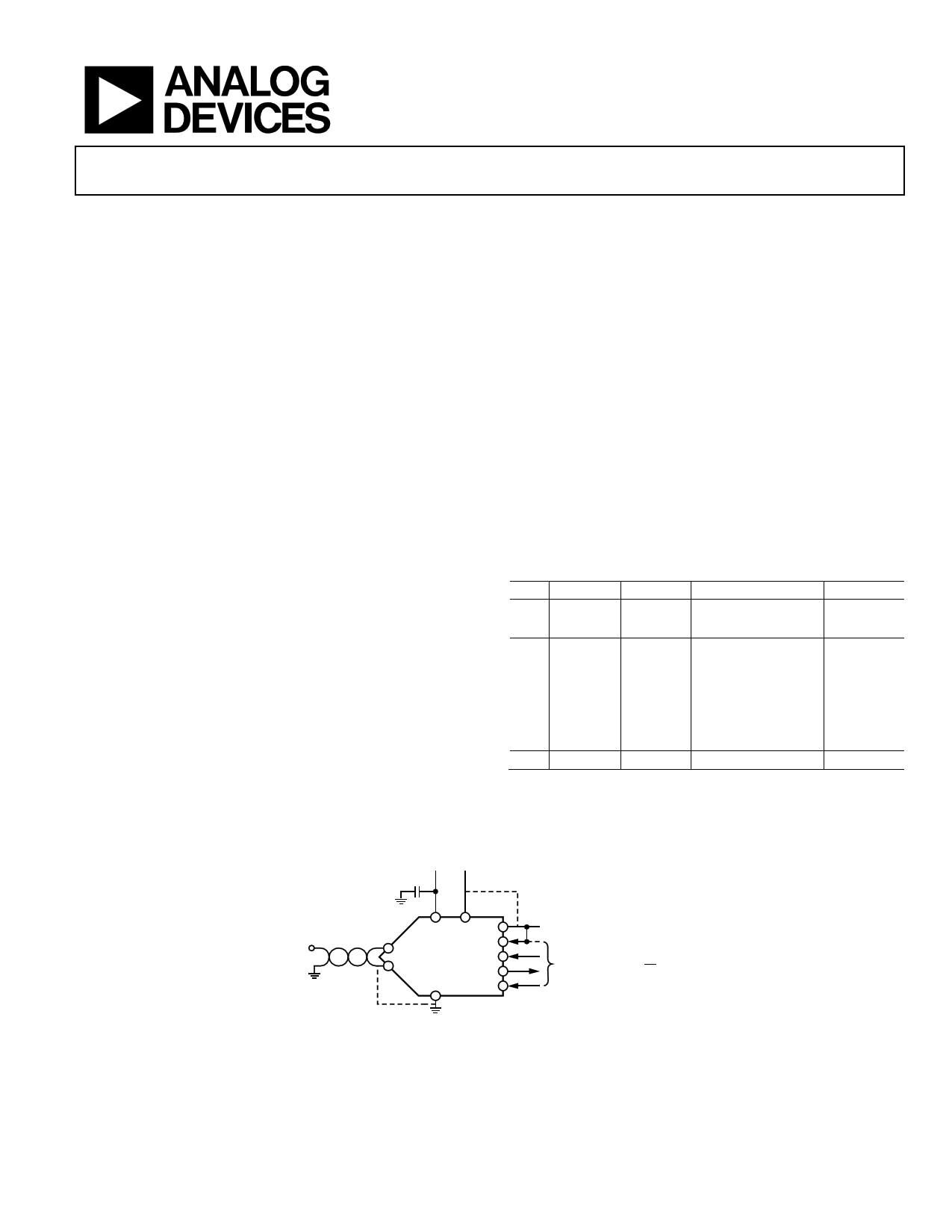
TYPICAL APPLICATION CIRCUIT
2.5V TO 5V 2.5V
0V TO VREF
REF VDD VIO
IN+ AD7988-1/ SDI
IN–
AD7988-5
SCK
SDO
GND
CNV
Figure 1.
1.8V TO 5.5V
3- OR 4-WIRE INTERFACE
(SPI, DAISY CHAIN, CS)
1 Protected by U.S. Patent 6,703,961.
Rev. F
Document Feedback
Information furnished by Analog Devices is believed to be accurate and reliable. However, no
responsibilityisassumedbyAnalogDevices for itsuse,nor foranyinfringementsofpatentsor other
rights of third parties that may result from its use. Specifications subject to change without notice. No
license is granted by implication or otherwise under any patent or patent rights of Analog Devices.
Trademarksandregisteredtrademarksarethepropertyoftheirrespectiveowners.
One Technology Way, P.O. Box 9106, Norwood, MA 02062-9106, U.S.A.
Tel: 781.329.4700 ©2012–2016 Analog Devices, Inc. All rights reserved.
Technical Support
www.analog.com
1 page 
Data Sheet
AD7988-1/AD7988-5
TIMING SPECIFICATIONS
VDD = 2.37 V to 2.63 V, VIO = 3.3 V to 5.5 V, −40°C to +125°C unless otherwise stated. See Figure 2 and Figure 3 for load conditions.
Table 4.
Parameter
AD7988-1
Throughput Rate
Conversion Time: CNV Rising Edge to Data Available
Acquisition Time
Time Between Conversions
AD7988-5
Throughput Rate
Conversion Time: CNV Rising Edge to Data Available
B Grade
C Grade
Acquisition Time
B Grade
C Grade
Time Between Conversions
CNV Pulse Width (CS Mode)
SCK Period (CS Mode)
VIO Above 4.5 V
VIO Above 3 V
VIO Above 2.7 V
VIO Above 2.3 V
SCK Period (Chain Mode)
VIO Above 4.5 V
VIO Above 3 V
VIO Above 2.7 V
VIO Above 2.3 V
SCK Low Time
SCK High Time
SCK Falling Edge to Data Remains Valid
SCK Falling Edge to Data Valid Delay
VIO Above 4.5 V
VIO Above 3 V
VIO Above 2.7 V
VIO Above 2.3 V
CNV or SDI Low to SDO D15 MSB Valid (CS Mode)
VIO Above 3 V
VIO Above 2.3V
CNV or SDI High or Last SCK Falling Edge to SDO High Impedance (CS Mode)
SDI Valid Setup Time from CNV Rising Edge
SDI Valid Hold Time from CNV Rising Edge (CS Mode)
SDI Valid Hold Time from CNV Rising Edge (Chain Mode)
SCK Valid Setup Time from CNV Rising Edge (Chain Mode)
SCK Valid Hold Time from CNV Rising Edge (Chain Mode)
SDI Valid Setup Time from SCK Falling Edge (Chain Mode)
SDI Valid Hold Time from SCK Falling Edge (Chain Mode)
Symbol Min
tCONV
tACQ
tCYC
tCONV
tACQ
tCYC
tCNVH
tSCK
tSCK
tSCKL
tSCKH
tHSDO
tDSDO
500
10
400
800
2
500
10.5
12
13
15
11.5
13
14
16
4.5
4.5
3
tEN
tDIS
tSSDICNV
tHSDICNV
tHSDICNV
tSSCKCNV
tHSCKCNV
tSSDISCK
tHSDISCK
5
2
0
5
5
2
3
Typ Max Unit
100 kHz
9.5 μs
ns
μs
500 kHz
1.6 µs
1.2 µs
ns
ns
μs
ns
ns
ns
ns
ns
ns
ns
ns
ns
ns
ns
ns
9.5 ns
11 ns
12 ns
14 ns
10 ns
15 ns
20 ns
ns
ns
ns
ns
ns
ns
ns
Rev. F | Page 5 of 23
5 Page 
Data Sheet
1.00
0.75
POSITIVE INL: +0.18 LSB
NEGATIVE INL: –0.21 LSB
0.50
0.25
0
–0.25
–0.50
–0.75
–1.00
0
16384
32768
49152
65536
CODE
Figure 12. Differential Nonlinearity vs. Code, VREF = 5 V
1.00
POSITIVE INL: +0.25 LSB
0.75
NEGATIVE INL: –0.22 LSB
0.50
0.25
0
–0.25
–0.50
–0.75
–1.00
0
16384
32768
49152
65536
CODE
Figure 13. Differential Nonlinearity vs. Code, VREF = 2.5 V
180k
160k
162595
140k
120k
100k
80k
60k 52720
42731
40k
20k
0 0 0 22 1291
852 29 2 0 0 0
8003 8004 8005 8006 8007 8008 8009 800A 800B 800C 800D 800E 800F
CODE IN HEX
Figure 14. Histogram of a DC Input at the Code Center, VREF = 5 V
AD7988-1/AD7988-5
60k
50970
50k
45198
40k
30k
20k 18848
12424
10k
2290
0 0 0 1 94
1217
30 0 0
7FFA 7FFB 7FFC 7FFD 7FFE 7FFF 8000 8001 8002 8003 8004 8005 8006
CODE IN HEX
Figure 15. Histogram of a DC Input at the Code Transition, VREF = 2.5 V
100
SNR
SINAD
ENOB
95
16
15
90 14
85 13
80 12
2.25 2.75 3.25 3.75 4.25 4.75 5.25
REFERENCE VOLTAGE (V)
Figure 16. SNR, SINAD, and ENOB vs. Reference Voltage
60k
53412
50k
40k
37417 31540
30k
20k
10k 7285
5807
0 0 0 19 590
512 11 0 0
7FFA 7FFB 7FFC 7FFD 7FFE 7FFF 8000 8001 8002 8003 8004 8005 8006
CODE IN HEX
Figure 17. Histogram of a DC Input at the Code Center, VREF = 2.5 V
Rev. F | Page 11 of 23
11 Page | ||
| Páginas | Total 23 Páginas | |
| PDF Descargar | [ Datasheet AD7988-5.PDF ] | |
Hoja de datos destacado
| Número de pieza | Descripción | Fabricantes |
| AD7988-1 | 16-Bit Lower Power PulSAR ADCs | Analog Devices |
| AD7988-5 | 16-Bit Lower Power PulSAR ADCs | Analog Devices |
| Número de pieza | Descripción | Fabricantes |
| SLA6805M | High Voltage 3 phase Motor Driver IC. |
Sanken |
| SDC1742 | 12- and 14-Bit Hybrid Synchro / Resolver-to-Digital Converters. |
Analog Devices |
|
DataSheet.es es una pagina web que funciona como un repositorio de manuales o hoja de datos de muchos de los productos más populares, |
| DataSheet.es | 2020 | Privacy Policy | Contacto | Buscar |