|
|
|
PDF CDP1851 Data sheet ( Hoja de datos )
| Número de pieza | CDP1851 | |
| Descripción | CMOS Programmable I/O Interface | |
| Fabricantes | GE | |
| Logotipo | ||
Hay una vista previa y un enlace de descarga de CDP1851 (archivo pdf) en la parte inferior de esta página. Total 12 Páginas | ||
|
No Preview Available !
_ _ _ _ _ _ _ _ _ _ _ _ _ _ _ _ _ _ _ _ _ _ _ _ _ _ _ _ _ _ CMOS Perlph~rals
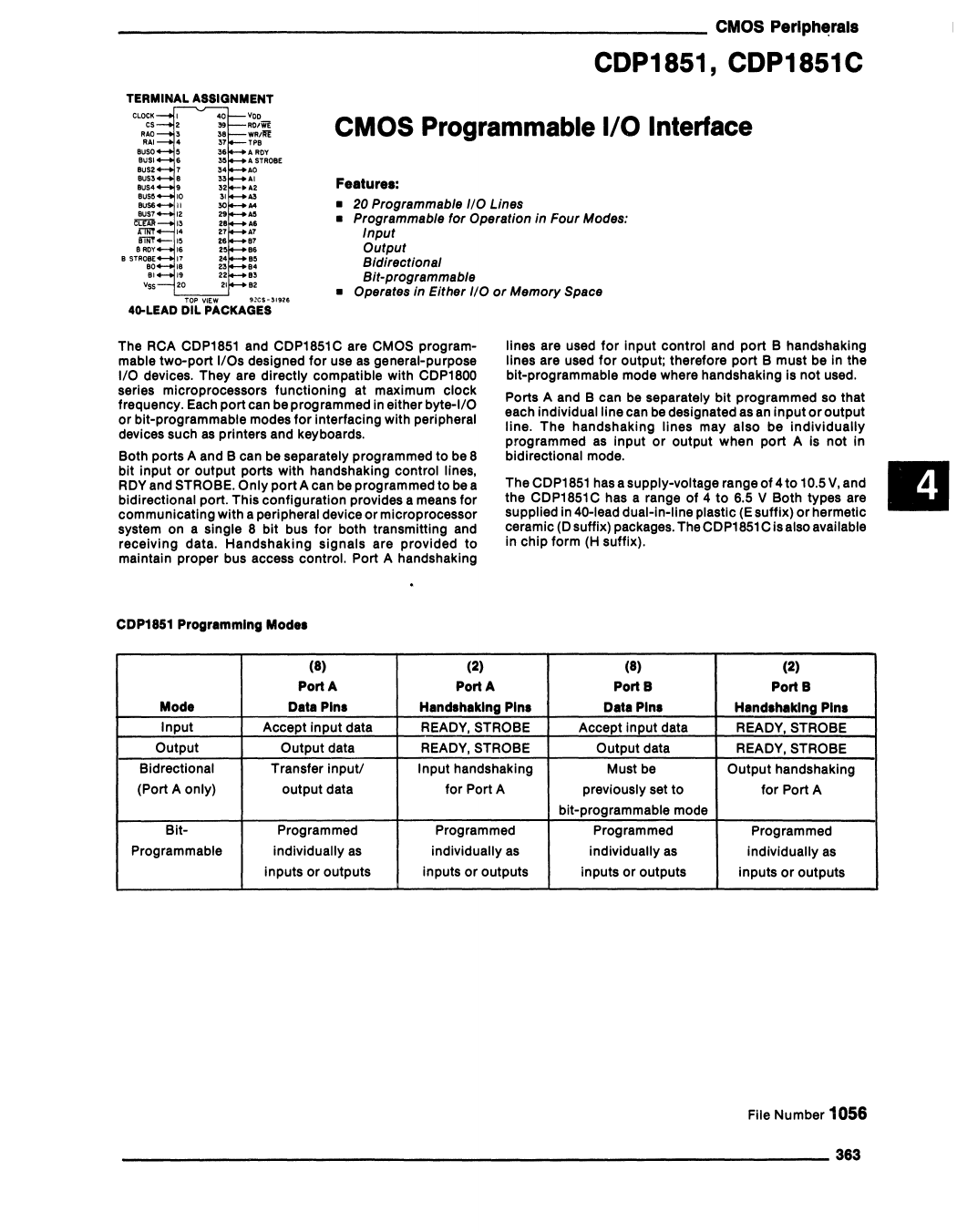
TERMINAL ASSIGNMENT
CL.OCI(
cs
RAD
RAI
BUSO
BUSI
BUS2
BUS3
BUS4
BUS5
.,.0e STROBE
VDD
RD/WE
".WR/liE
A ROY
A STROBE
AD
AI
.A2
A3
A4
All
...A6
.7A7
•.•,,
V55 .2
TOP VIEW
9~CS~31926
4G-LEAO OIL PACKAGES
CDP1851, CDP1851C
CMOS Programmable 1/0 Interface
Features:
• 20 Programmable 110 Lines
• Programmable for Operation in Four Modes:
Input
Output
Bidirectional
Bit-programmable
• Operates in Either I/O or Memory Space
The RCA CDP1851 and CDP1851C are CMOS program-
mable two-port I/Os designed for use as general-purpose
1/0 devices. They are directly compatible with CDP1800
series microprocessors functioning at maximum clock
frequency. Each port can be programmed in either byte-I/O
or bit-programmable modes for interfacing with peripheral
devices such as printers and keyboards.
Both ports A and B can be separately programmed to be 8
bit input or output ports with handshaking control lines,
ROY and STROBE. Only port A can be programmed to be a
bidirectional port. This configuration provides a means for
communicating with a peripheral device or microprocessor
system on a single 8 bit bus for both transmitting and
receiving data. Handshaking signals are provided to
maintain proper bus access control. Port A handshaking
lines are used for input control and port B handshaking
lines are used for output; therefore port B must be in the
bit-programmable mode where handshaking is not used.
Ports A and B can be separately bit programmed so that
each individual line can be designated as an input or output
line. The handshaking lines may also be individually
programmed as input or output when port A is not in
bidirectional mode.
The CDP1851 has a supply-voltage range of 4 to 10.5 V, and
the CDP1851C has a range of 4 to 6.5 V Both types are
supplied in 40-lead dual-in-line plastic (E suffix) or hermetic
ceramic (0 suffix) packages. The CDP1851 C is also available
in chip form (H suffix).
CDP1851 Progrsmmlng Modes
Mode
Input
Output
Bidrectional
(Port A only)
(8)
PortA
Dala Pins
Accept input data
Output data
Transfer input!
output data
Bit-
Programmable
Programmed
individually as
inputs or outputs
(2)
PortA
Handshaking Pins
READY, STROBE
READY, STROBE
Input handshaking
for Port A
Programmed
individually as
inputs or outputs
(8)
Port B
Dala Pins
Accept input data
Output data
Must be
previously set to
bit-programmable mode
Programmed
individually as
inputs or outputs
(2)
Port B
Handshaking Pins
READY, STROBE
READY, STROBE
Output handshaking
for Port A
Programmed
individually as
inputs or outputs
File Number 1056
____________________________________________________________ 363
1 page 
CMOS Peripherals
CDP1851, CDP1851 C
PROGRAMMING
1. Initialization and Control.
TI!!..QPP1851 PIO must be cleared by a low on the
CLEAR Input during power-on to set ilfor programming.
Once programmed, modes can be changed without
clearing except wh~ing the bit-programmable
mode. A low on the CLEAR input sets both ports to the
input modes, disables interrupts, unmasks all bit-
programmed interrupt bits, and resets the status
register, A ROY, and B ROY.
2. Mode SeUlng
The control register must be sequentially loaded with
the appropriate mode set control bytes in order as
shown in table I (i.e. input mode then output mode,
etc.). Port A is set with the SET A bit = 1 and port Bisset
with the SET B bit = 1. If a port is set to the bit-
programmable mode, the bit-programming control byte
from table II must be loaded. A bit is programmed for
output with the 1/0 bit =1 and for input with the 1/0 bit =
O. The STROBE and ROY lines may be programmed for
input or output with the STROBEIROY control byte of
table II. Input data on the STROBE and ROY lines is
detected by reading the status register. When using the
STROBE or ROY lines for output. the control byte must
be loaded every time output data is to be changed. To
program logical conditions that will generate an
interrupt, the interrupt control byte of table III must be
loaded. An interrupt mask of the eight 1/0 lines may be
loaded next, if bit 04 (mask follows) of the interrupt
control byte = 1. The 1/0 lines are masked if the
corresponding bit of the interrupt mask register is 1,
otherwise it is monitored. Any combination of masked
bits are permissable, except all bits masked (mask =
FF).
3. INT Eneble/Dlaable
To enable or disable the INT line in all modes, the
interrupt ENABLEIOISABLE byte must be loaded (see
Table IV). Interrupts can also be detected by reading
the status register see table V. All interrupts should be
disabled when programming or false interrupts may
occur. The INT outputs are open drain NMOS devices
that allow wired ORing (use 10K pull-up registers).
A FLOW CHART GUIDE TO CDP1851 MODE PROGRAMMING
lEI
NO
REPEAT FOR EACH
BIT-PROGRAMMABLE
PORT
SET MASTER INTERUPT
ENABLE I DISABLE
USING TABLE Dr
REPEAT FOR EACH
BIT- PROGRAMMABLE
PORT
NOTES
I. STROBE I READY :I/O CONTROL BYTE (TABLE I I I
IS ALSO USED TO OUTPUT DATA TO STROBE AND
READY LINES WHEN BIT-PROGRAMMED.
2· STATUS REGISTER (TABLE III IS USED TO
INPUT DATA FROM STROBE AND READY LINES
WHEN BIT-PROGRAMMED·
3.INTERRUPT STATUS IS ALSO READ FROM
STATUS REGISTER.
92CM- 34508
____________________________________________________________ 367
5 Page 
_ _ _ _ _ _ _ _ _ _ _ _ _ _ _ _ _ _ _ _ _ _ _ _ _ _ _ CMOS Peripherals
CDP1851, CDP1851C
OYNAMIC ELECTRICAL CHARACTERISTICS al TA = -40 10 +850 C, VOO ± 5'10,
Ir, II = 20 ns, VIH = 0.7 VOO, VIL = 0.3 VOO, CL = 100 pF
CHARACTERISTIC
VOO
(V)
LIMITS
COP1851
COP1851C
Min. Typ.- Max.+ Min. Typ.- Max.+
UNITS
Oulpul Mode see Figs. 4 and 6
Minimum Setup Times:
Chip Select to CLOCK
-RO/WE to CLOCK
WR/RE to CLOCK
Address to WRITE'
Data Bus to WRITE'
Minimum Hold Times:
Chip Select After CLOCK
Address After WRITE'
Data Bus After WRITE'
Propagation Delay Times:
WRITE • to Data Out
-
WRITE' to INT
WRITE' to RDY
STROBE to INT
STROBE to RDY
Minimum Pulse Widths:
CLOCK
STROBE
WRITE'
tCSCl
tRWCl
5
10
5
10
-
-
-
-
-50 75
-25 40
75 120 -
-40 60
tWRCl
5
10
5
-
-
-
75 120 -
40 60 -
50 75 -
tAW 10 -
25 40 -
tDW
tHCSCl
5
10
5
10
-
-
-
-
80 120 -
40 60 -
75 120 -
-40 60
5-
tHAW 10 -
5-
50 75 -
-25 40
-50 75
tHDW 10 -
25 40 -
5
-
225 350
-
tWDO 10 -
125 200
-
tWINT
5
10
-
-
300 450
150 225
-
-
5
-
350 525
-
tWRDY 10
-
175 275
-
5
-
200 300
-
-tSTINT 10
100 150
-
5 260 400
tSTRDY 10
-
130 200
-
-5 75 120 -
-tWCl
10
40 60 -
5
-
100 150
-
tWST 10 -
5-
50 75
175 275
-
-
tww 10 -
90 150 -
• WRITE is the overlap of RD/WE =0 and WR/RE =1.
-Typical values are for TA = 25 0 C and nominal voltages.
+Maximum limits of minimum characteristics are the values above which all devices function.
50 75
--
75 120
--
75 120
--
50 75
--
80 120
--
75 120
--
50 75
--
50 75
--
225 350
--
300 450
--
350 525
--
200 300
--
260 400
--
75 120
--
100 150
--
175 275
--
ns
..
_ _ _ _ _ _ _ _ _ _ _ _ _ _ _ _ _ _ _ _ _ _ _ _ _ _ _ _ _ _ _ _ 373
11 Page | ||
| Páginas | Total 12 Páginas | |
| PDF Descargar | [ Datasheet CDP1851.PDF ] | |
Hoja de datos destacado
| Número de pieza | Descripción | Fabricantes |
| CDP1851 | CMOS Programmable I/O Interface | Intersil Corporation |
| CDP1851 | CMOS Programmable I/O Interface | GE |
| CDP1851C | CMOS Programmable I/O Interface | Intersil Corporation |
| CDP1851C | CMOS Programmable I/O Interface | GE |
| Número de pieza | Descripción | Fabricantes |
| SLA6805M | High Voltage 3 phase Motor Driver IC. |
Sanken |
| SDC1742 | 12- and 14-Bit Hybrid Synchro / Resolver-to-Digital Converters. |
Analog Devices |
|
DataSheet.es es una pagina web que funciona como un repositorio de manuales o hoja de datos de muchos de los productos más populares, |
| DataSheet.es | 2020 | Privacy Policy | Contacto | Buscar |