|
|
|
PDF HMC7044 Data sheet ( Hoja de datos )
| Número de pieza | HMC7044 | |
| Descripción | 14-Output Jitter Attenuator | |
| Fabricantes | Analog Devices | |
| Logotipo | ||
Hay una vista previa y un enlace de descarga de HMC7044 (archivo pdf) en la parte inferior de esta página. Total 30 Páginas | ||
|
No Preview Available !
Data Sheet
High Performance, 3.2 GHz, 14-Output
Jitter Attenuator with JESD204B
HMC7044
FEATURES
Ultralow rms jitter: 44 fs typical (12 kHz to 20 MHz) at
2457.6 MHz
Noise floor: −156 dBc/Hz at 2457.6 MHz
Low phase noise: −141.7 dBc/Hz at 800 kHz, 983.04 MHz output
Up to 14 LVDS, LVPECL, or CML type device clocks (DCLKs)
from PLL2
Maximum CLKOUTx/CLKOUTx and SCLKOUTx/SCLKOUTx
frequency up to 3200 MHz
JESD204B-compatible system reference (SYSREF) pulses
25 ps analog, and ½ VCO cycle digital delay independently
programmable on each of 14 clock output channels
SPI-programmable phase noise vs. power consumption
SYSREF valid interrupt to simplify JESD204B synchronization
Narrow-band, dual core VCOs
Up to 2 buffered voltage controlled oscillator (VCXO) outputs
Up to 4 input clocks in LVDS, LVPECL, CMOS, and CML modes
Frequency holdover mode to maintain output frequency
Loss of signal (LOS) detection and hitless reference switching
4× GPIOs alarms/status indicators to determine the health of
the system
External VCO input to support up to 6000 MHz
On-board regulators for excellent PSRR
68-lead, 10 mm × 10 mm LFCSP package
APPLICATIONS
JESD204B clock generation
Cellular infrastructure (multicarrier GSM, LTE, W-CDMA)
Data converter clocking
Microwave baseband cards
Phase array reference distribution
GENERAL DESCRIPTION
The HMC7044 is a high performance, dual-loop, integer-N
jitter attenuator capable of performing reference selection and
generation of ultralow phase noise frequencies for high speed data
converters with either parallel or serial (JESD204B type) interfaces.
The HMC7044 features two integer mode PLLs and overlapping
on-chip VCOs that are SPI-selectable with wide tuning ranges
around 2.5 GHz and 3 GHz, respectively. The device is designed
to meet the requirements of GSM and LTE base station designs,
and offers a wide range of clock management and distribution
features to simplify baseband and radio card clock tree designs.
The HMC7044 provides 14 low noise and configurable outputs
to offer flexibility in interfacing with many different compo-
nents including data converters, field-programmable gate arrays
(FPGAs), and mixer local oscillators (LOs).
The DCLK and SYSREF clock outputs of the HMC7044 can be
configured to support signaling standards, such as CML, LVDS,
LVPECL, and LVCMOS, and different bias settings to offset
varying board insertion losses.
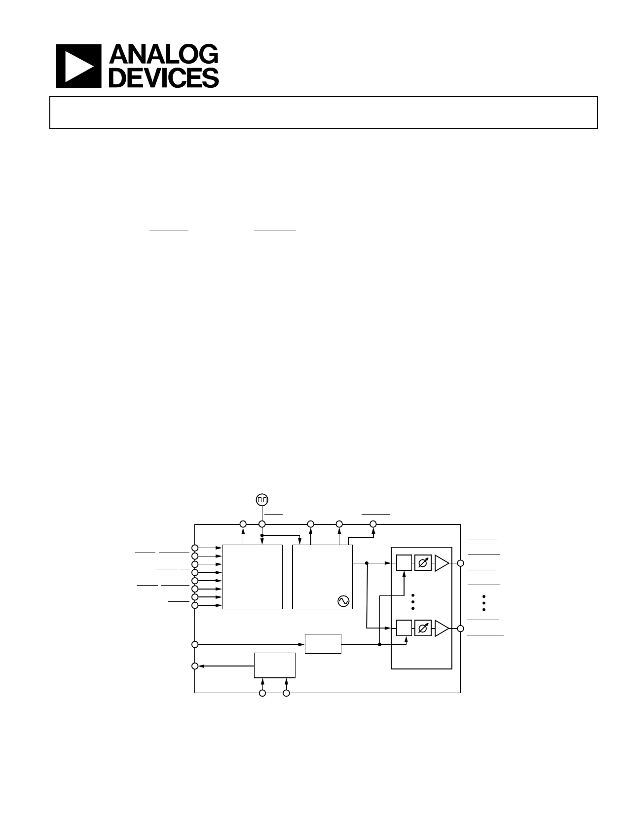
FUNCTIONAL BLOCK DIAGRAM
CLKIN0/RFSYNCIN
CLKIN0/RFSYNCIN
CLKIN1/FIN
CLKIN1/FIN
CLKIN2/OSCOUT0
CLKIN2/OSCOUT0
CLKIN3
CLKIN3
SYNC
SDATA
OSCIN
CPOUT1 OSCIN
CPOUT2 OSCOUT1 OSCOUT1
PLL1
PLL2
÷
CLKOUT0
CLKOUT0
SCLKOUT1
SCLKOUT1
CLKOUT2
CLKOUT2
SCLKOUT3
SCLKOUT3
SPI
CONTROL
INTERFACE
SYSREF
CONTROL
÷
14-CLOCK
DISTRIBUTION
CLKOUT12
CLKOUT12
SCLKOUT13
SCLKOUT13
SLEN SCLK
Figure 1.
Rev. B
Document Feedback
Information furnished by Analog Devices is believed to be accurate and reliable. However, no
responsibilityisassumedbyAnalogDevices for itsuse,nor foranyinfringementsofpatentsor other
rights of third parties that may result from its use. Specifications subject to change without notice. No
license is granted by implication or otherwise under any patent or patent rights of Analog Devices.
Trademarksandregisteredtrademarksarethepropertyoftheirrespectiveowners.
One Technology Way, P.O. Box 9106, Norwood, MA 02062-9106, U.S.A.
Tel: 781.329.4700 ©2015–2016 Analog Devices, Inc. All rights reserved.
Technical Support
www.analog.com
1 page 
HMC7044
Data Sheet
DIGITAL INPUT/OUTPUT (I/O) ELECTRICAL SPECIFICATIONS
Table 3.
Parameter
DIGITAL INPUT SIGNALS (RESET, SYNC, SLEN, SCLK)
Safe Input Voltage Range1
Input Load
Input Voltage
Input Logic High (VIH)
Input Logic Low (VIL)
SPI Bus Frequency
DIGITAL BIDIRECTIONAL SIGNALS CONFIGURED AS
INPUTS (SDATA, GPIO4, GPIO3, GPIO2, GPIO1)
Safe Input Voltage Range1
Input Capacitance
Input Resistance
Input Voltage
Input Logic High (VIH)
Input Logic Low (VIL)
Input Hysteresis
GPIO1 TO GPIO4 ALARM MUXING/DELAY
Delay from Internal Alarm/Signal to General-Purpose
Output (GPO) Driver
DIGITAL BIDIRECTIONAL SIGNALS CONFIGURED AS
OUTPUTS (SDATA, GPIO4, GPIO3, GPIO2, GPIO1)
CMOS MODE
Logic 1 Level
Logic 0 Level
Output Drive Resistance (RDRIVE)
Output Driver Delay (tDGPO)
Maximum Supported DC Current1
OPEN-DRAIN MODE1
Logic 1 Level
Logic 0 Level
Pull-Down Impedance
Maximum Supported Sink Current
Min Typ
−0.1
0.3
1.2
0
−0.1
0.4
50G
1.22
0
0.2
2
Max Unit Test Conditions/Comments
+3.6 V
pF
VCC V
0.5 V
10 MHz
+3.6 V
pF
Ω
VCC V
0.24 V
V
ns
Occurs around 0.85 V
Does not include tDGPO
1.6 1.9
2.2 V
0 0.1 V
50 Ω
1.5 + 42 ×
CLOAD
ns Approximately 1.5 ns + 0.69 × RDRIVE × CLOAD
(CLOAD in nF)
0.6 mA
External 1 kΩ pull-up resistor
3.6 V
3.6 V maximum permitted; specifications
set by external supply
0.13
0.28 V
Against a 1 kΩ external pull-up resistor to
3.3 V
60 Ω
5 mA
1 Guaranteed by design and characterization.
Rev. B | Page 4 of 72
5 Page 
HMC7044
Data Sheet
SPUR CHARACTERISTICS
Table 8.
Parameter
REFERENCE SPUR PERFORMANCE
At 122.88 MHz and Its Harmonics
Min Typ Max Unit Test Conditions/Comments
−70 dBc
NOISE AND JITTER CHARACTERISTICS
Table 9.
Parameter
CLOSED-LOOP PHASE NOISE—WIDE LOOP FILTER
SSB Phase Noise
At 2457.6 MHz1
At 614.4 MHz1
CLOSED-LOOP PHASE NOISE—NARROW LOOP FILTER
SSB Phase Noise
At 2949.12 MHz2
At 983.04 MHz2
Min Typ
Max Unit
Test Conditions/Comments
For best integrated noise
−98.0
−111.1
−119.8
−125.2
−126.9
−131.3
−150.0
−154.0
−156.3
44.0
−110.4
−122.8
−131.3
−136.6
−138.3
−142.7
−157.6
−158.8
−159.2
50.0
dBc/Hz
dBc/Hz
dBc/Hz
dBc/Hz
dBc/Hz
dBc/Hz
dBc/Hz
dBc/Hz
dBc/Hz
fs
Offset = 100 Hz
Offset = 1 kHz
Offset = 10 kHz
Offset = 100 kHz
Offset = 300 kHz
Offset = 1 MHz
Offset = 5 MHz
Offset = 10 MHz
Offset = 100 MHz
Integrated jitter = 12 kHz to 20 MHz
dBc/Hz
dBc/Hz
dBc/Hz
dBc/Hz
dBc/Hz
dBc/Hz
dBc/Hz
dBc/Hz
dBc/Hz
fs
Offset = 100 Hz
Offset = 1 kHz
Offset = 10 kHz
Offset = 100 kHz
Offset = 300 kHz
Offset = 1 MHz
Offset = 5 MHz
Offset = 10 MHz
Offset = 100 MHz
Integrated jitter = 12 kHz to 20 MHz
For best 800 kHz offset
−100.9
−103.8
−106.9
−109.9
−132.3
−134.5
−152
−155.3
108
−110.4
−113.3
−116.4
−119.4
−141.7
−143.7
−157.1
Rev. B | Page 10 of 72
dBc/Hz
dBc/Hz
dBc/Hz
dBc/Hz
dBc/Hz
dBc/Hz
dBc/Hz
dBc/Hz
fs
Offset = 100 Hz
Offset = 1 kHz
Offset = 10 kHz
Offset = 100 kHz
Offset = 800 kHz
Offset = 1 MHz
Offset = 10 MHz
Offset = 100 MHz
Integrated jitter = 12 kHz to 20 MHz
dBc/Hz
dBc/Hz
dBc/Hz
dBc/Hz
dBc/Hz
dBc/Hz
dBc/Hz
Offset = 100 Hz
Offset = 1 kHz
Offset = 10 kHz
Offset = 100 kHz
Offset = 800 kHz
Offset = 1 MHz
Offset = 10 MHz
11 Page | ||
| Páginas | Total 30 Páginas | |
| PDF Descargar | [ Datasheet HMC7044.PDF ] | |
Hoja de datos destacado
| Número de pieza | Descripción | Fabricantes |
| HMC7043 | 14-Output Fanout Buffer | Analog Devices |
| HMC7044 | 14-Output Jitter Attenuator | Analog Devices |
| HMC704LP4E | 8 GHZ FRACTIONAL-N PLL | Hittite Microwave Corporation |
| Número de pieza | Descripción | Fabricantes |
| SLA6805M | High Voltage 3 phase Motor Driver IC. |
Sanken |
| SDC1742 | 12- and 14-Bit Hybrid Synchro / Resolver-to-Digital Converters. |
Analog Devices |
|
DataSheet.es es una pagina web que funciona como un repositorio de manuales o hoja de datos de muchos de los productos más populares, |
| DataSheet.es | 2020 | Privacy Policy | Contacto | Buscar |