|
|
|
PDF HMC787A Data sheet ( Hoja de datos )
| Número de pieza | HMC787A | |
| Descripción | Fundamental Mixer | |
| Fabricantes | Analog Devices | |
| Logotipo | ||
Hay una vista previa y un enlace de descarga de HMC787A (archivo pdf) en la parte inferior de esta página. Total 18 Páginas | ||
|
No Preview Available !
Data Sheet
GaAs, MMIC, Fundamental Mixer,
3 GHz to 10 GHz
HMC787A
FEATURES
Conversion loss: 9 dB typical at 3 GHz to 9 GHz
Local oscillator (LO) to radio frequency (IF) isolation:
43 dB typical at 3 GHz to 9 GHz
RF to intermediate frequency (IF) isolation: 26 dB typical at
3 GHz to 9 GHz
Input third-order intercept (IP3): 24 dBm typical at
3 GHz to 9 GHz
Input 1 dB compression point (P1dB): 17 dBm typical at
3 GHz to 9 GHz
Input second-order intercept (IP2): 67 dBm typical at
3 GHz to 9 GHz
Passive double-balanced topology
Wide IF frequency range: dc to 4 GHz
12-terminal, ceramic, leadless chip carrier (LCC) package
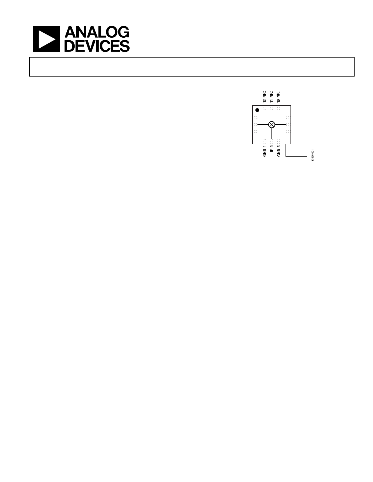
FUNCTIONAL BLOCK DIAGRAM
GND 1
LO 2
GND 3
HMC787A
9 GND
8 RF
7 GND
PACKAGE
BASE
GND
Figure 1.
APPLICATIONS
Microwave radio
Industrial, scientific, and medical (ISM) band and ultrawide
band (UWB) radio
Test equipment and sensors
Military end use
GENERAL DESCRIPTION
The HMC787A is a general-purpose, double balanced mixer in
a 12-terminal, RoHS compliant, ceramic leadless chip carrier
(LCC) package that can be used as an upconverter or down-
converter from 3 GHz to 10 GHz. This mixer is fabricated in a
gallium arsenide (GaAs), metal semiconductor field effect
transistor (MESFET) process and requires no external components
or matching circuitry. The HMC787A provides excellent local
oscillator (LO) to radio frequency (RF) and LO to intermediate
frequency (IF) isolation due to optimized balun structures and
operates with a LO drive level of 17 dBm. The ceramic LCC
package eliminates the need for wire bonding and is compatible
with high volume, surface-mount manufacturing techniques.
Rev. A
Document Feedback
Information furnished by Analog Devices is believed to be accurate and reliable. However, no
responsibilityisassumedbyAnalogDevices for itsuse,nor foranyinfringementsofpatentsor other
rights of third parties that may result from its use. Specifications subject to change without notice. No
license is granted by implication or otherwise under any patent or patent rights of Analog Devices.
Trademarksandregisteredtrademarksarethepropertyoftheirrespectiveowners.
One Technology Way, P.O. Box 9106, Norwood, MA 02062-9106, U.S.A.
Tel: 781.329.4700 ©2016–2017 Analog Devices, Inc. All rights reserved.
Technical Support
www.analog.com
1 page 
HMC787A
ABSOLUTE MAXIMUM RATINGS
Table 2.
Parameter
RF Input Power
LO Input Power
IF Input Power
IF Source and Sink Current
Continuous Power Dissipation, PDISS
(TA = 85°C, Derate 11.6 mW/°C Above 85°C)
Maximum Junction Temperature
Maximum Peak Reflow Temperature (MSL3)1
Operating Temperature Range
Storage Temperature Range
Electrostatic Discharge (ESD) Sensitivity
Human Body Model (HBM)
Field Induced Charged Device Model
(FICDM)
Rating
28 dBm
28 dBm
28 dBm
12 mA
1044 mW
175°C
260°C
−40°C to +85°C
−65°C to +150°C
1500 V (Class 1C)
1000 V (Class C5)
1 See the Ordering Guide section.
Stresses at or above those listed under Absolute Maximum
Ratings may cause permanent damage to the product. This is a
stress rating only; functional operation of the product at these
or any other conditions above those indicated in the operational
section of this specification is not implied. Operation beyond
the maximum operating conditions for extended periods may
affect product reliability.
Data Sheet
THERMAL RESISTANCE
Thermal performance is directly linked to printed circuit board
(PCB) design and operating environment. Careful attention to
PCB thermal design is required.
Table 3. Thermal Resistance
Package Type
θJA
E-12-11
120
θJC
86
Unit
°C/W
1 See JEDEC standard JESD51-2 for additional information on optimizing the
thermal impedance (PCB with 3 × 3 vias).
ESD CAUTION
Rev. A | Page 4 of 17
5 Page 
HMC787A
Data Sheet
UPCONVERTER PERFORMANCE
Data taken as upconverter, lower sideband (high-side LO), TA = 25°C, and LO drive level = 17 dBm, unless otherwise noted.
Measurements taken with LO amplifier in line with lab bench LO source.
0
–2 +85°C
+25°C
–4 –40°C
–6
–8
–10
–12
–14
–16
–18
–20
3 4 5 6 7 8 9 10 11
RF FREQUENCY (GHz)
Figure 30. Conversion Gain vs. RF Frequency for Various Temperatures,
IF = 100 MHz, LO Power = 17 dBm
0
–2
15dBm
17dBm
–4
19dBm
21dBm
–6
–8
–10
–12
–14
–16
–18
–20
3 4 5 6 7 8 9 10 11
RF FREQUENCY (GHz)
Figure 33. Conversion Gain vs. RF Frequency for Various LO Powers,
IF = 100 MHz, Temperature = 25°C
50
45 +85°C
+25°C
40 –40°C
35
30
25
20
15
10
5
0
3 4 5 6 7 8 9 10 11
RF FREQUENCY (GHz)
Figure 31. Input Third-Order Intercept (IP3) vs. RF Frequency for Various
Temperatures, IF = 100 MHz, LO Power = 17 dBm
50
45
15dBm
17dBm
40
19dBm
21dBm
35
30
25
20
15
10
5
0
3 4 5 6 7 8 9 10 11
RF FREQUENCY (GHz)
Figure 34. Input Third-Order Intercept (IP3) vs. RF Frequency for Various LO
Powers, IF = 100 MHz, Temperature = 25°C
0
–2 +85°C
+25°C
–4 –40°C
–6
–8
–10
–12
–14
–16
–18
–20
3 4 5 6 7 8 9 10 11
RF FREQUENCY (GHz)
Figure 32. Conversion Gain vs. RF Frequency for Various Temperatures,
IF = 1100 MHz, LO Power = 17 dBm
0
–2 13dBm
15dBm
–4 17dBm
19dBm
–6 21dBm
–8
–10
–12
–14
–16
–18
–20
3 4 5 6 7 8 9 10 11
RF FREQUENCY (GHz)
Figure 35. Conversion Gain vs. RF Frequency for Various LO Powers,
IF = 1100 MHz, Temperature = 25°C
Rev. A | Page 10 of 17
11 Page | ||
| Páginas | Total 18 Páginas | |
| PDF Descargar | [ Datasheet HMC787A.PDF ] | |
Hoja de datos destacado
| Número de pieza | Descripción | Fabricantes |
| HMC787A | Fundamental Mixer | Analog Devices |
| HMC787LC3B | GaAs MMIC FUNDAMENTAL MIXER | Hittite Microwave |
| Número de pieza | Descripción | Fabricantes |
| SLA6805M | High Voltage 3 phase Motor Driver IC. |
Sanken |
| SDC1742 | 12- and 14-Bit Hybrid Synchro / Resolver-to-Digital Converters. |
Analog Devices |
|
DataSheet.es es una pagina web que funciona como un repositorio de manuales o hoja de datos de muchos de los productos más populares, |
| DataSheet.es | 2020 | Privacy Policy | Contacto | Buscar |