|
|
PDF NJM2749A Data sheet ( Hoja de datos )
| Número de pieza | NJM2749A | |
| Descripción | Low Drift Dual JFET Input Operational Amplifier | |
| Fabricantes | New Japan Radio | |
| Logotipo |  |
|
Hay una vista previa y un enlace de descarga de NJM2749A (archivo pdf) en la parte inferior de esta página. Total 12 Páginas | ||
|
No Preview Available !
NJM2749/2749A
Low Offset, Low Drift Dual JFET Input Operational Amplifier
■GENRRAL DESCRIPTION
The NJM2749/2749A is a Precision dual JFET input operational
amplifier which includes low input offset voltage: 0.8mV (typ) / 2.5mV
(max) and 6µV/°C typical offset drift.
The NJM2749A is guaranteed 20µV/°C maximum offset drift to
perform a 100% tested.
The NJM2749/2749A have the following features: low bias current of
50pA (typ), high slew rate of 13V/µs (typ).
These features are suitable for signal processing amplifiers of
instrumentation, measurement and industrial applications such as
sensor amplifier, current sensing and sample-and-hold circuit.
■ PACKAGE OUTLINE
NJM2749D / 2749AD
( DIP8 )
NJM2749M / 2749AM
( DMP8 )
■FEATURES
●Input Offset Voltage Drift
●Input Offset Voltage
●Input Bias Current
●Slew Rate
●Operating Voltage
●Voltage Gain
●Bipolar Technology
●Dual channel
●Package Outline
NJM2749: ∆VIO/∆T= 6µV/°C typ.
NJM2749A: ∆VIO/∆T=20µV/°C max.
2.5mV max. @Ta=25°C ~ 85°C
3.5mV max. @Ta= -40°C
IB= 50pA typ. 200pA max. @Ta=25°C
SR=13V/µs typ. @Ta=25°C
Vopr= ±6.0V ~ ±16V
Av=100dB typ.
NJM2749E / 2749AE
( SOP8 )
NJM2749D, NJM2749AD : DIP8
NJM2749M, NJM2749AM : DMP8
NJM2749E, NJM2749AE : SOP8 JEDEC 150mil
■PIN CONFIGURATION
OUTPUT A 1
−INPUT A 2
+INPUT A 3
V− 4
(Top View)
A
B
8 V+
7 OUTPUT B
6 −INPUT B
5 +INPUT B
NJM2749/2749A
Ver.2009-01-13
-1-
1 page 
NJM2749/2749A
■IMPORTANT CONSIDERATIONS FOR USE OF NJM2749/2749A
•THE OSCILLATION WITH A CAPACITIVE LOAD
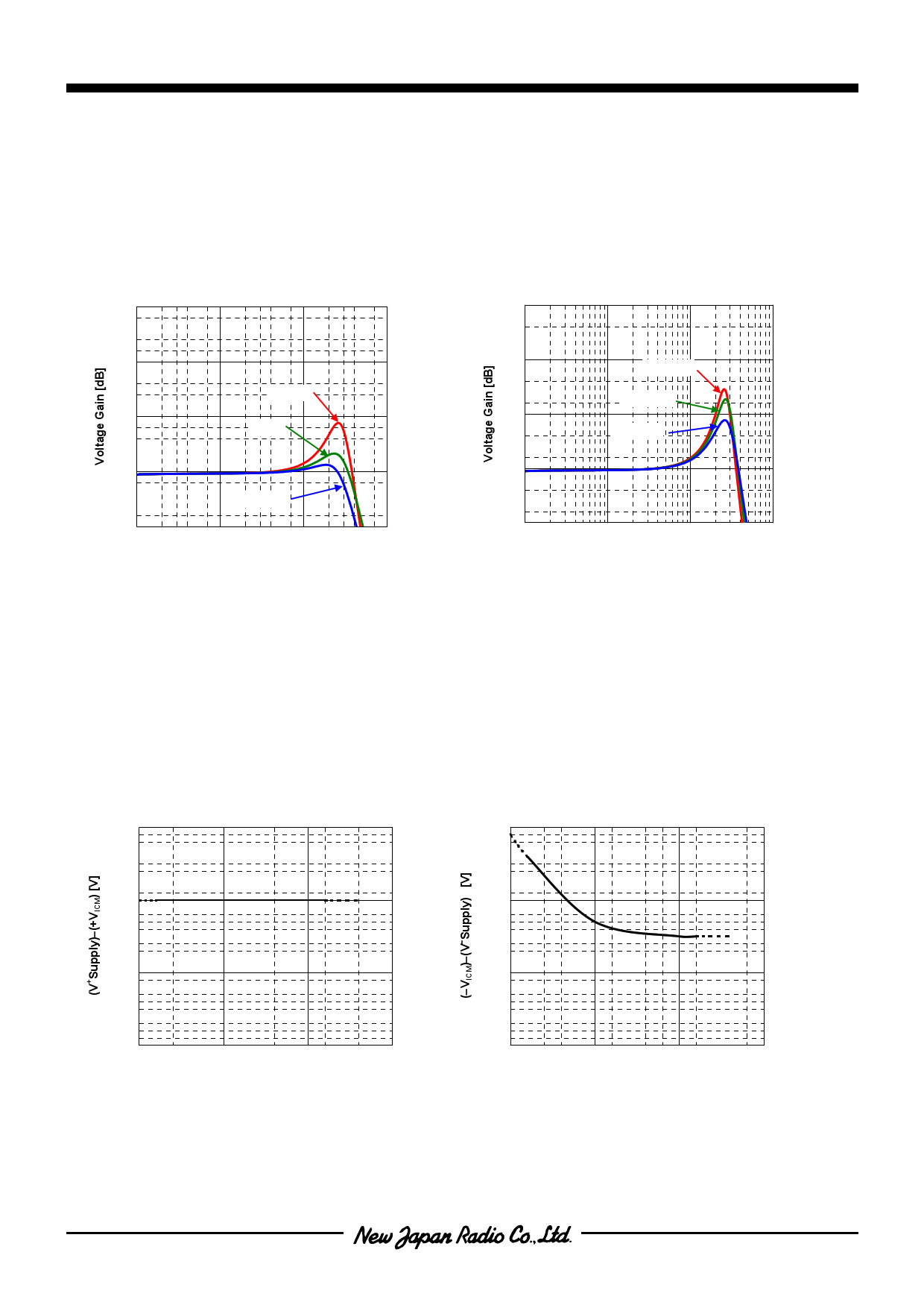
NJM2749/2749A tends to oscillate easily when it uses voltage-follower, and driving capacitive load.
The figure below is a “Voltage Gain - Frequency characteristic” in the Voltage-Follower. (It is not the one to guarantee the
characteristic of the product.)
Especially, it becomes easy to oscillate in the condition that the input voltage (output voltage) is near the minus supply voltage
side and the condition with large output sink current. We will recommend use by some circuit gains.
Voltage Gain − Frequency
(V+/V−=±15V, Voltage Follower,
15 CL=100pF, ISINK=1mA, Ta=25ºC)
Voltage Gain − Frequency
(V+/V−=±15V, Voltage Follower,
15 CL=100pF, VO=−10V, Ta=25ºC)
10
VO=-10V
5
VO=0V
10 ISINK=5mA
ISINK=2mA
5
ISINK=1mA
00
VO=+10V
-5
10k
100k
1010M0k
Frequency [HZ]
10100M0k
-5
10k
100k
1010M0k
Frequency [HZ]
10100M0k
•INPUT COMMON MODE VOLTAGE RANGE
In this product, the input offset voltage drift is measured based on the input offset voltage at VICM=0V, and the input voltage
range that satisfies the common mode rejection ratio 76dB is defined as the input common mode voltage range.
As an electric characteristic, VICM=−10V~+10V at Supply Voltage V+/V−=±15V is guaranteed.
It becomes below formula about the input common mode voltage range when the supply voltage changes.
+VICM:
−VICM:
(V+
(V−
supply)
supply)
−
+
5
5
[V]
[V]
·
·
·
·
·
·
reference
reference
This figure below is “Input common mode voltage range – Supply voltage characteristics”. (It is not the one to guarantee the
characteristic of the product.)
+ VICM is limited by the absolute maximum rating (V+ supply) within the input common mode voltage range.
Moreover, −VICM tends to rise by lowering of the supply voltage.
Common Mode Input Voltage Range (+VICM)
− Supply Voltage
(Ta=25ºC, CMR=76dB)
1.0
Common Mode Input Voltage Range (−VICM)
− Supply Voltage
(Ta=25ºC, CMR=76dB)
5.0
0.0 4.0
-1.0 3.0
-2.0
5
10 15
Supply Voltage V+/V− [V]
20
2.0
5
10 15
Supply Voltage V+/V− [V]
20
•OTHERS
For the NJM2749/2749A are high-precision products, a surface leak by dirt and/or condensation on package can have a
detrimental effect on precise characteristics of these products.
You should pay close attention to environment of storage and usage.
Ver.2008-01-13
-5-
5 Page 
■TYPICAL CHARACTERISTICS
Slew Rate − Ambient Temperature
20 (V+/V−=±15V, Voltage Follower, VO=±1V, RL=2kΩ)
15
+SR
10 -SR
5
-50
-25 0 25 50 75 100 125
Ambient Temperature [ºC]
THD+N − Output Voltage
1 (RF=9kΩ, V+/V−=±15V, AV=+10, RL=open, Ta=25ºC)
0.1
0.01
0.001
0.01
20kHz
1kHz
20Hz
0.1 1
Output Voltage VO [Vrms]
10
THD+N − Frequency
1 (RF=9kΩ, V+/V−=±15V, AV=+10, RL=open, Ta=25ºC)
0.1
0.01
0.001
01k0
VO=7.07Vrms
VO=5Vrms
100k0 1k 10k
Frequency [Hz]
100k
Ver.2008-01-13
NJM2749/2749A
Slew Rate − Supply Voltage
(Voltage Follower, VO=±1V, RL=2kΩ, Ta=25ºC)
20
15 +SR
-SR
10
5
5 10 15 20
Supply Voltage V+/V− [V]
THD+N − Output Voltage
1 (RF=1.8kΩ, V+/V−=±15V, AV=+10, RL=open, Ta=25ºC)
20kHz
0.1
1kHz
0.01
0.001
0.01
20Hz
0.1 1
Output Voltage VO [Vrms]
10
THD+N − Frequency
1 (RF=1.8kΩ, V+/V−=±15V, AV=+10, RL=open, Ta=25ºC)
0.1
VO=7.07Vrms
0.01
0.001
01k0
VO=5Vrms
100k0 1k 10k
Frequency [Hz]
100k
- 11 -
11 Page | ||
| Páginas | Total 12 Páginas | |
| PDF Descargar | [ Datasheet NJM2749A.PDF ] | |
Hoja de datos destacado
| Número de pieza | Descripción | Fabricantes |
| NJM2749 | Low Drift Dual JFET Input Operational Amplifier | New Japan Radio |
| NJM2749A | Low Drift Dual JFET Input Operational Amplifier | New Japan Radio |
| Número de pieza | Descripción | Fabricantes |
| SLA6805M | High Voltage 3 phase Motor Driver IC. |
Sanken |
| SDC1742 | 12- and 14-Bit Hybrid Synchro / Resolver-to-Digital Converters. |
Analog Devices |
|
DataSheet.es es una pagina web que funciona como un repositorio de manuales o hoja de datos de muchos de los productos más populares, |
| DataSheet.es | 2020 | Privacy Policy | Contacto | Buscar |
