|
|
PDF NJG1156PCD Data sheet ( Hoja de datos )
| Número de pieza | NJG1156PCD | |
| Descripción | GPS Front-End Module | |
| Fabricantes | New Japan Radio | |
| Logotipo |  |
|
Hay una vista previa y un enlace de descarga de NJG1156PCD (archivo pdf) en la parte inferior de esta página. Total 20 Páginas | ||
|
No Preview Available !
NJG1156PCD
GPS Front-End Module
I GENERAL DESCRIPTION
The NJG1156PCD is a front-end module (FEM) designed for GPS
applications. The NJG1156PCD offers high gain, low noise figure, high
linearity and very high out-band rejection characteristics brought by included
high performance pre- SAW filter, low noise amplifier (LNA) and post- SAW
filter. The NJG1156PCD can be operated from 1.5V to 3.3V single voltage.
The NJG1156PCD offers very small mounting area by included two SAW
filters, only two external components and very small HFFP10-CD package
that is 2.5x2.5mm.
I PACKAGE OUTLINE
NJG1156PCD
I FEATURES
G Low supply voltage
1.8/ 2.8V typ.
G Low current consumption
2.6/3.3mA typ. @VDD=1.8/ 2.8V, VCTL=1.8V
G High gain
G Low noise figure
0.1µA typ.
@VDD=1.8/ 2.8V, VCTL=0V (Stand-by mode)
17.5/18.5dB typ. @VDD=1.8/ 2.8V, VCTL=1.8V, f=1575MHz
1.60/1.55dB typ. @VDD=1.8/ 2.8V, VCTL=1.8V, f=1575MHz
G High out band rejection
85dBc typ.
@f=704 to 915MHz, relative to 1575MHz
75dBc typ.
@f=1710 to 1980MHz, relative to 1575MHz
78dBc typ.
@f=1526 to 1536MHz, 1627 to 1680MHz,
relative to 1575MHz
G Small package size
HFFP10-CD: 2.5mmx2.5mmx0.63mm max.
G RoHS compliant and Halogen Free, MSL1
I PIN CONFIGURATION
(Top View)
1
Post-Filter
GND
VCTL
2
VDD LNA
3
NC(GND)
4
PreIN
5
Pre-Filter
I BLOCK DIAGRAM
10
PostOUT
NC (GND)
9
LNAIN
8
PreOUT
7
GND
6
Pin connection
1. GND
2. VCTL
3. VDD
4. NC(GND)
5. PreIN
6. GND
7. PreOUT
8. LNAIN
9. NC(GND)
10. PostOUT
RF IN
Exposed pad: GND
Pre-Filter
VCTL
VDD
LNA
Post-Filter RF OUT
I TRUTH TABLE
“H”=VCTL(H), “L”=VCTL(L)
VCTL
Mode
H Active mode
L Stand-by mode
Note: Specifications and description listed in this datasheet are subject to change without notice.
Ver.2016-04-25
-1-
1 page 
NJG1156PCD
I TERMINAL INFORMATION
No. SYMBOL
DESCRIPTION
1
GND
Ground terminal. This terminal should be connected to the ground plane as
close as possible for excellent RF performance.
2 VCTL Control voltage terminal.
3
VDD
Supply voltage terminal. Please connect bypass capacitor C1 with ground as
close as possible.
4
NC(GND)
No connected terminal. This terminal is not connected with internal circuit.
Please connect to the PCB ground Plane.
5 PreIN RF input terminal. This terminal connects to input of pre-SAW filter.
6
GND
Ground terminal. This terminal should be connected to the ground plane as close
as possible for excellent RF performance.
7 PreOUT Pre-SAW filter output terminal. This terminal connects to LNAIN with L1.
8
9
10
Exposed
Pad
LNAIN
RF input terminal. This terminal requires only a matching inductor L1, and
does not require DC blocking capacitor because of integrated capacitor.
NC(GND)
PostOUT
No connected terminal. This terminal is not connected with internal circuit.
Please connect to the PCB ground Plane.
RF output terminal. This terminal requires no DC blocking capacitor since this
terminal has integrated SAW that also works as DC blocking capacitor in
nature.
GND Ground terminal.
-5-
5 Page 
NJG1156PCD
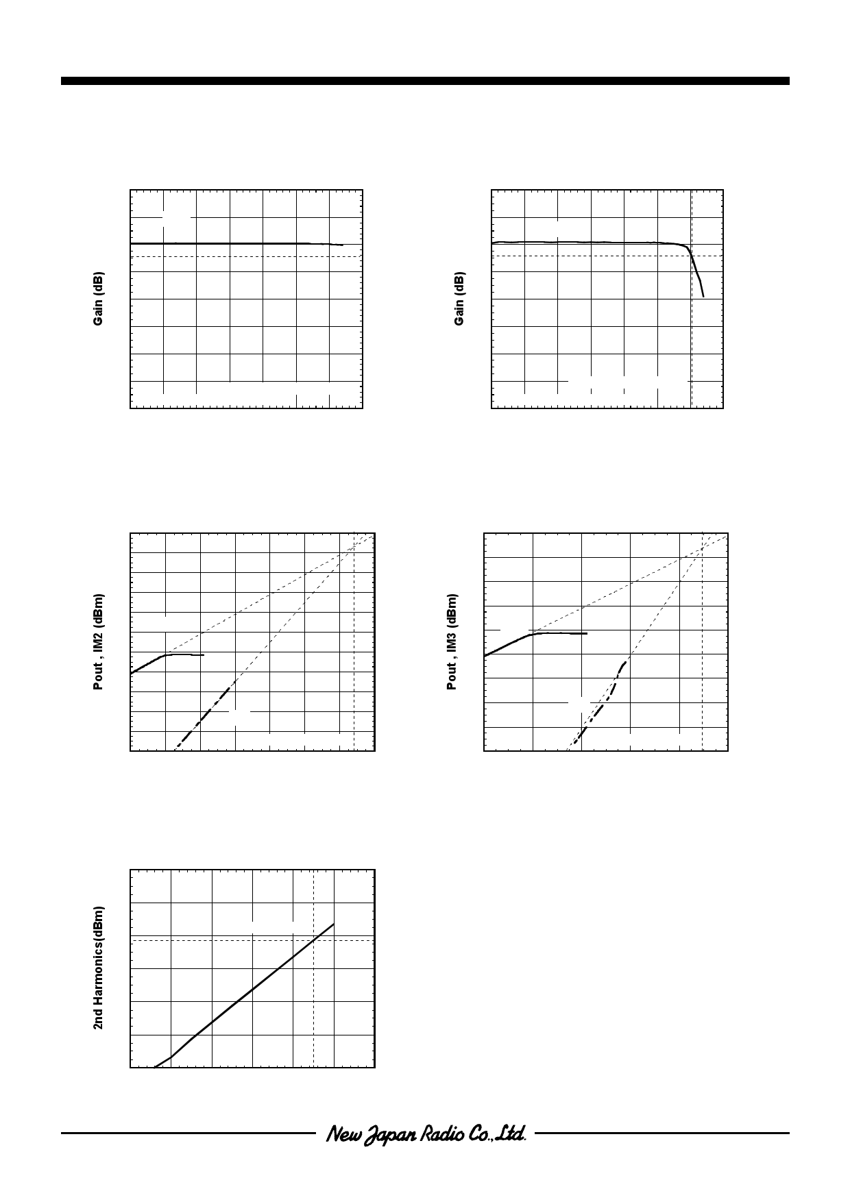
I ELECTRICAL CHARACTERISTICS
Conditions: VDD=1.8V, VCTL=1.8V, Ta=25°C, Zs=Zl=50Ω, with application circuit
Out-of-band P-1dB (fjam=900MHz)
(VDD=1.8V, VCTL=1.8V, f =1575MHz at Pin=-40dBm)
22 meas
Out-of-band P-1dB (fjam=1710MHz)
(VDD=1.8V,
22
V CTL=1.8V,
f =1575MHz
meas
at
Pin=-40dBm)
20 Gain
18
20
Gain
18
16 16
14 14
12 12
10 10
8
P-1dB(IN)_OB > +24.0dBm
(Gain: Exclude PCB, Connector Losses)
6
-40 -30 -20 -10 0
10 20
Pin at 900MHz (dBm)
30
8 P-1dB(IN)_OB = +20.5dBm
(Gain: Exclude PCB, Connector Losses)
6
-40 -30 -20 -10 0
10 20
Pin at 1710MHz (dBm)
30
Out-of-band IIP2
(V =1.8V, V =1.8V, f =1575.4MHz,
DD CTL meas
120 f1=824.6MHz, f2=2400MHz)
100
80
60
40
Pout
20
0
-20
-40
-60
-80
-100
-40
-20
IM2
IIP2_OB=+87.8dBm
0 20 40 60
Pin (dBm)
80
100
2nd Harmonics
(V =1.8V, V =1.8V,
DD CTL
fin=787.76MHz, f =1575.52MHz)
0 meas
-20
2fo=-42.7dBm
-40
-60
-80
-100
-120
-30 -20 -10
0
10
Pin(dBm)
20
30
Out-of-band IIP3
(VDD=1.8V, V CTL=1.8V, fmeas=1575.4MHz,
f1=1712.7MHz, f2=1850MHz)
80
60
40
20
0 Pout
-20
-40
-60
-80
-100
-40
IM3
IIP3_OB=+49.5dBm
-20 0 20 40
Pin (dBm)
60
- 11 -
11 Page | ||
| Páginas | Total 20 Páginas | |
| PDF Descargar | [ Datasheet NJG1156PCD.PDF ] | |
Hoja de datos destacado
| Número de pieza | Descripción | Fabricantes |
| NJG1156PCD | GPS Front-End Module | New Japan Radio |
| Número de pieza | Descripción | Fabricantes |
| SLA6805M | High Voltage 3 phase Motor Driver IC. |
Sanken |
| SDC1742 | 12- and 14-Bit Hybrid Synchro / Resolver-to-Digital Converters. |
Analog Devices |
|
DataSheet.es es una pagina web que funciona como un repositorio de manuales o hoja de datos de muchos de los productos más populares, |
| DataSheet.es | 2020 | Privacy Policy | Contacto | Buscar |
