|
|
|
PDF HMC877LC3 Data sheet ( Hoja de datos )
| Número de pieza | HMC877LC3 | |
| Descripción | BROADBAND TIME DELAY & PHASE SHIFTER | |
| Fabricantes | Analog Devices | |
| Logotipo | ||
Hay una vista previa y un enlace de descarga de HMC877LC3 (archivo pdf) en la parte inferior de esta página. Total 15 Páginas | ||
|
No Preview Available !
HMC877LC3
v03.0614
BROADBAND TIME DELAY & PHASE SHIFTER
SMT, 8 - 23 GHz
Typical Applications
The HMC877LC3 is ideal for:
• Synchronization of clock and data
• Transponder design
• Broadband Test & Measurement
• RF ATE Applications
Features
Very Wide Bandwidth: 8 - 23 GHz
Continuous Adjustable Delay Range: 500° (1.4 UI[1])
Single-Ended or Differential Operation
Adjustable Differential Output Voltage
Swing: 500 - 950 mVp-p @ 16 GHz
Delay Control Modulation Bandwidth: 2.5 GHz
Single Supply: +3.3V
16 Lead Ceramic 3x3mm SMT Package: 9mm²
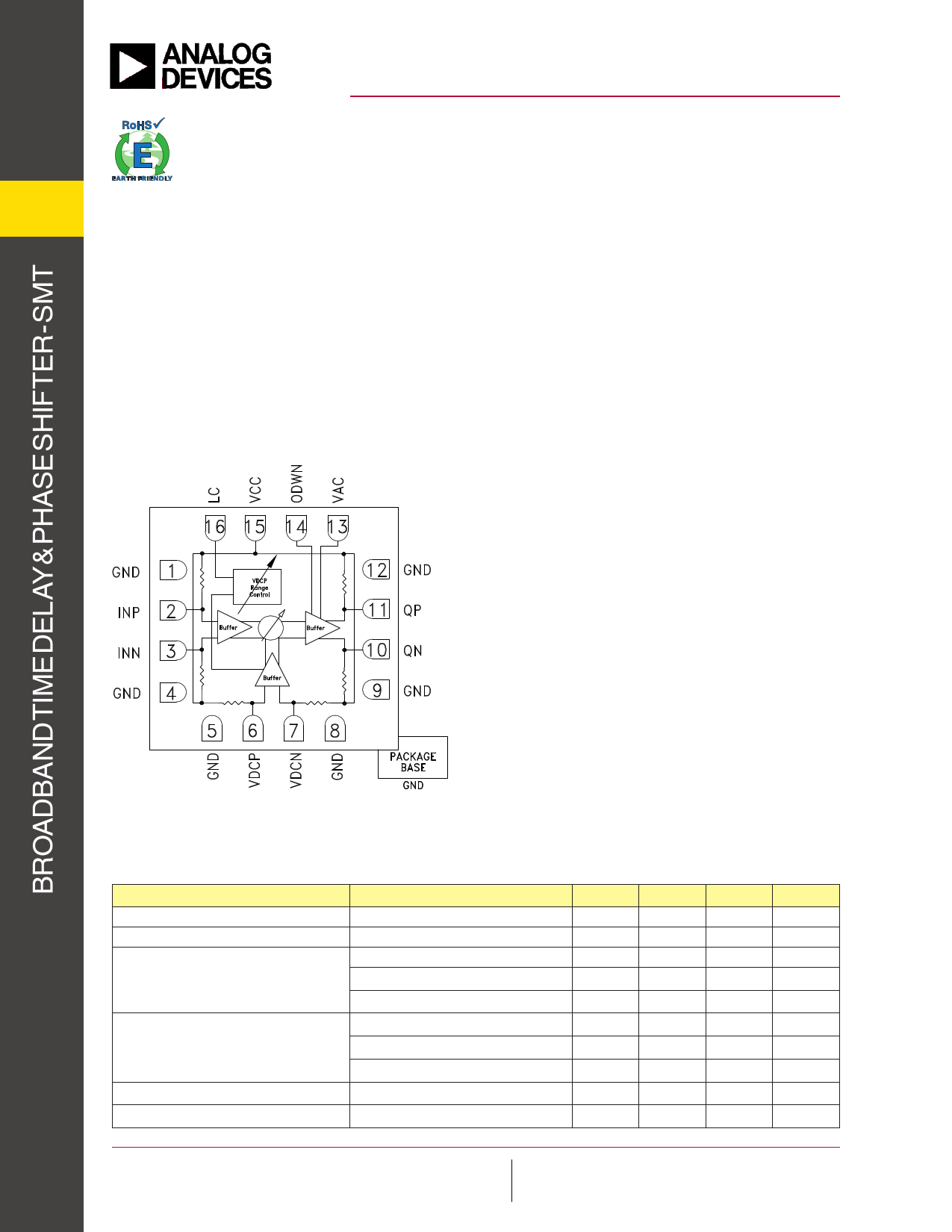
Functional Diagram
General Description
The HMC877LC3 is a phase shifter/time delay with
0 to 500°(1.4 UI) continuously adjustable shift/delay
range. The delay control is linearly monotonic with
respect to the differential control voltage (VDCP,
VDCN) and the control input has a modulation band-
width of 2.5 GHz. The device provides a differential
output voltage with constant amplitude for single-
ended or differential input voltages above the input
sensitivity level, while the output voltage swing may be
adjusted using the VAC control pin. The HMC877LC3
features internal temperature compensation and bias
circuitry to minimize delay variations with temperature.
The device also features a delay control voltage range
adjustment pin, LC. All RF input and outputs of the
HMC877LC3 are internally terminated with 50 Ohms
to Vcc, and may either be AC or DC coupled. Output
pins can be connected directly to a 50 Ohm to Vcc
terminated system, while DC blocking capacitors must
be used if the terminated system input is 50 Ohms to a
DC voltage other than Vcc. The HMC877LC3 is avail-
able in ROHS-compliant 3x3 mm SMT package.
Electrical Specifications, TA = +25° C, Vcc = 3.3V, GND=ODWN = 0V
Parameter
Conditions
Min.
Typ.
Max.
Units
Power Supply Voltage
Power Supply Current
± %5 Tolerance
ODWN = 0V
@ 10 GHz
3.135 3.3 3.465
V
175 190 215 mA
504 Deg
Phase Shift Range
@ 16 GHz
498 Deg
@ 22 GHz
485 Deg
@ 10 GHz
1.4 UI
Time Delay Range
@ 16 GHz
1.38
UI
@ 22 GHz
1.35
UI
Delay Control Modulation Bandwidth
2.5 GHz
Delay Control Voltage (VDCP)
[1] The UI stands for unit interval
VCC-0.6
VCC+0.6
V
1 IrrlTiniecgrfaseohFpdntrseomsoemnoarsfatiisibtrophkingislrirrtdayafiuncnpirsdtnaeeairdrste,sihegsbesduiysdmtteheimebarledtypidvmlbiAcetyaranPayArtadioyrlhnoeenamgsolauooanlDrgtnrkeofeDrsdvtoh:eiamcevrt9eAreicowist7etspihssipe8usepfsop-lbeularr2.neioicdtSlcp5iseepeaevu0rreetstcya-deioinofo3,iycfrtnno3atdophtria4eboeSftienoer3rsrnursaetasspc:noupcyrbpeHujipcernFoaatcifirttvttareieetnttnoixg:aottecnew:rPmhdign9aeeMhhnrn7rtegssotls.8eiiaocnobwf-frel2Aiepoth:n.5aowatH9ue0lotona7g-wntsv38oDeotevi3e-crev2eo7riC,.ct5h3eNneos0oor.r-p3oFOPA3Oohprn4arrope3dntlpiTieecorei:aorcnc7treihO,8o,n1n2naod-S3lp-eoE2lulgpiil9vpniysez-pe4rW@aoy7arb,a0hty:tae0i,Pntwt•Ptdhhi.wOtoOetDnor.w.decrB:epi.ovo1hrlax-emoi8ctn9,et0l1iCi0tn0oe-eh6rA.d,ceaNeNtolArmwosmL:rwOswAfwGoono.-aardDdlno,a,gMloMADgAe.0cv2oi0c0me16s28,-29In410c.6,
1 page 
HMC877LC3
v03.0614
BROADBAND TIME DELAY & PHASE SHIFTER
SMT, 8 - 23 GHz
Phase Shift vs. Control Voltage
@ VDCP=2.7V to 3.9V with 0.1V step [1][2][3]
550
500
450
400
350
300
250
200
150
100
50
0
8
9 10 11 12 13 14 15 16 17 18 19 20 21 22 23
FREQUENCY (GHz)
Phase Shift vs. Temperature @VDCP=3.3V
(Relative to VDCP=VCC-0.6V) [1][2]
340
320
300
280
260
240
220
200
8
9 10 11 12 13 14 15 16 17 18 19 20 21 22 23
FREQUENCY (GHz)
+25 C
+85 C
-40 C
Phase Error vs. Control Voltage
@ Fmean=16 GHz [1][2][3][4]
15
10
Phase Shift vs. Control Voltage
@ 10 GHz [1][2][3][4]
12
8
54
00
-5 -4
-10
-15
8
9 10 11 12 13 14 15 16 17 18 19 20 21 22 23
FREQUENCY (GHz)
VDCP-VDCN=-0.6 V
VDCP-VDCN=-0.4 V
VDCP-VDCN=-0.2 V
VDCP-VDCN= 0 V
VDCP-VDCN= 0.2 V
VDCP-VDCN= 0.4 V
VDCP-VDCN= 0.6 V
Phase Shift vs. Control Voltage
@ 22 GHz [1][2][3][4]
30
-8
-12
-15
-12.5
-10 -7.5
Pin (dBm)
VDCP-VDCN=-0.6V
VDCP-VDCN=-0.2V
VDCP-VDCN=-0.1V
VDCP-VDCN= 0V
-5 -2.5
0
VDCP-VDCN= 0.2V
VDCP-VDCN= 0.4V
VDCP-VDCN= 0.6V
DC Current vs. Temperature [2][5]
250
20 225
10 200
0 175
-10 150
-20 125
-30
-15
-12.5
-10 -7.5
Pin (dBm)
VDCP-VDCN=-0.6V
VDCP-VDCN=-0.2V
VDCP-VDCN=-0.1V
VDCP-VDCN= 0V
-5 -2.5 0
VDCP-VDCN= 0.2V
VDCP-VDCN= 0.4V
VDCP-VDCN= 0.6V
100
3.135
3.218 3.3 3.383
SUPPLY VOLTAGE (V)
+25 C
+85 C
-40 C
3.465
[1] VCC = 3.3V [2] ODWN= 0 V, VDCN=VCC
[4] VDCP-VDCN=-0.6V is taken as reference level
[3] 25°C
[5] VDCP=3.3V and input frequency is 20 GHz
IrrlTiniecgrfaseohFpdntrseomsoemnoarsfatiisibtrophkingislrirrtdayafiuncnpirsdtnaeeairdrste,sihegsbesduiysdmtteheimebarledtypidvmlbiAcetyaranPayArtadioyrlhnoeenamgsolauooanlDrgtnrkeofeDrsdvtoh:eiamcevrt9eAreicowist7etspihssipe8usepfsop-lbeularr2.neioicdtSlcp5iseepeaevu0rreetstcya-deioinofo3,iycfrtnno3atdophtria4eboeSftienoer3rsrnursaetasspc:noupcyrbpeHujipcernFoaatcifirttvttareieetnttnoixg:aottecnew:rPmhdign9aeeMhhnrn7rtegssotls.8eiiaocnobwf-frel2Aiepoth:n.5aowatH9ue0lotona7g-wntsv38oDeotevi3e-crev2eo7riC,.ct5h3eNneos0oor. r-p3oFOPA3Oohprn4arrope3dntlpiTieecorei:aorcnc7treihO,8o,n1n2naod-S3lp-eoE2lulgpiil9vpniysez-pe4rW@aoy7arb,a0hty:tae0i,Pntwt•Ptdhhi.wOtoOetDnor.w.decrB:epi.ovo1hrlax-emoi8ctn9,et0l1iCi0tn0oe-eh6rA.d,ceaNeNtolArmwosmL:rwOswAfwGoono.-aardDdlno,a,gMloMADgAe.0cv2oi0c0me16s28,-29In410c.6,
4
5 Page 
Outline Drawing
HMC877LC3
v03.0614
BROADBAND TIME DELAY & PHASE SHIFTER
SMT, 8 - 23 GHz
NOTES:
1. PACKAGE BODY MATERIAL: ALUMINA
2. LEAD AND GROUND PADDLE PLATING: 30-80 MICROINCHES GOLD OVER 50 MICRO-
INCHES MINIMUM NICKEL.
3. DIMENSIONS ARE IN INCHES [MILLIMETERS].
4. LEAD SPACING TOLERANCE IS NON-CUMULATIVE.
5. CHARACTERS TO BE BLACK INK MARKED WITH .018”MIN to .030”MAX HEIGHT
REQUIREMENTS. UTILIZE MAXIMUM CHARACTER HEIGHT BASED ON LID DIMENSIONS
AND BEST FIT. LOCATE APPROX. AS SHOWN.
6. PACKAGE WARP SHALL NOT EXCEED 0.05mm DATUM -C-
7. ALL GROUND LEADS AND GROUND PADDLE MUST BE SOLDERED TO PCB RF
GROUND.
Package Information
Part Number
Package Body Material
HMC877LC3
Alumina, White
[1] Max peak reflow temperature of 260 °C
[2] 4-Digit lot number XXXX
Lead Finish
Gold over Nickel
MSL Rating
MSL3 [1]
Package Marking [2]
H877
XXXX
IrrlTiniecgrfaseohFpdntrseomsoemnoarsfatiisibtrophkingislrirrtdayafiuncnpirsdtnaeeairdrste,sihegsbesduiysdmtteheimebarledtypidvmlbiAcetyaranPayArtadioyrlhnoeenamgsolauooanlDrgtnrkeofeDrsdvtoh:eiamcevrt9eAreicowist7etspihssipe8usepfsop-lbeularr2.neioicdtSlcp5iseepeaevu0rreetstcya-deioinofo3,iycfrtnno3atdophtria4eboeSftienoer3rsrnursaetasspc:noupcyrbpeHujipcernFoaatcifirttvttareieetnttnoixg:aottecnew:rPmhdign9aeeMhhnrn7rtegssotls.8eiiaocnobwf-frel2Aiepoth:n.5aowatH9ue0lotona7g-wntsv38oDeotevi3e-crev2eo7riC,.ct5h3eNneos0oor. r-p3oFOPA3Oohprn4arrope3dntlpiTieecorei:aorcnc7treihO,8o,n1n2naod-S3lp-eoE2lulgpiil9vpniysez-pe4rW@aoy7arb,a0hty:tae0i,Pntwt•Ptdhhi.wOtoOetDnor.w.decrB:epi.ovo1hrlax-emoi8ctn9,et0l1iCi0tn0oe-eh6rA.d,ceaNeNtolArmwosmL:rwOswAfwGoono.-aardDdlno,a,gMloMADgAe.0cv2oi0c0me16s28,-29In410c.6,
10
11 Page | ||
| Páginas | Total 15 Páginas | |
| PDF Descargar | [ Datasheet HMC877LC3.PDF ] | |
Hoja de datos destacado
| Número de pieza | Descripción | Fabricantes |
| HMC877LC3 | BROADBAND TIME DELAY & PHASE SHIFTER | Analog Devices |
| Número de pieza | Descripción | Fabricantes |
| SLA6805M | High Voltage 3 phase Motor Driver IC. |
Sanken |
| SDC1742 | 12- and 14-Bit Hybrid Synchro / Resolver-to-Digital Converters. |
Analog Devices |
|
DataSheet.es es una pagina web que funciona como un repositorio de manuales o hoja de datos de muchos de los productos más populares, |
| DataSheet.es | 2020 | Privacy Policy | Contacto | Buscar |