|
|
|
PDF CAT28F002 Data sheet ( Hoja de datos )
| Número de pieza | CAT28F002 | |
| Descripción | 2 Megabit CMOS Boot Block Flash Memory | |
| Fabricantes | Catalyst Semiconductor | |
| Logotipo | ||
Hay una vista previa y un enlace de descarga de CAT28F002 (archivo pdf) en la parte inferior de esta página. Total 16 Páginas | ||
|
No Preview Available !
CAT28F002
2 Megabit CMOS Boot Block Flash Memory
Licensed Intel
second source
FEATURES
s Fast Read Access Time: 90/120/150 ns
s On-Chip Address and Data Latches
s Blocked Architecture:
— One 16-KB Protected Boot Block
• Top or Bottom Locations
— Two 8-KB Parameter Blocks
— One 96-KB Main Block
— One 128-KB Main Block
s Hardware Data Protection
s Automated Program and Erase Algorithms
s Automatic Power Savings Feature
s Low Power CMOS Operation
s 12.0V ± 5% Programming and Erase Voltage
DESCRIPTION
s Electronic Signature
s 100,000 Program/Erase Cycles and 10 Year
Data Retention
s Standard Pinouts:
— 40-Lead TSOP
— 40-Lead PDIP
s High Speed Programming
s Commercial, Industrial and Automotive Tem-
perature Ranges
s Reset/Deep PowerDown Mode
— 0.2µA ICC Typical
— Acts as Reset for Boot Operations
The CAT28F002 is a high speed 256K X 8-bit electrically
erasable and reprogrammable Flash memory ideally
suited for applications requiring in-system or after sale
code updates.
The CAT28F002 has a blocked architecture with one 16
KB Boot Block, two 8 KB Parameter Blocks, one 96 KB
Main Block and one 128 KB Main Block. The Boot Block
section can be at the top or bottom of the memory map.
The Boot Block section includes a reprogramming write
lock out feature to guarantee data integrity. It is de-
signed to contain secure code which will bring up the
system minimally and download code to other locations
of CAT28F002.
The CAT28F002 is designed with a signature mode
which allows the user to identify the IC manufacturer and
device type. The CAT28F002 is also designed with on-
Chip Address Latches, Data Latches, Programming and
Erase Algorithms. A deep power-down mode lowers the
total Vcc power consumption 1µw typical.
The CAT28F002 is manufactured using Catalyst’s ad-
vanced CMOS floating gate technology. It is designed
to endure 100,000 program/erase cycles and has a data
retention of 10 years. The device is available in JEDEC
approved 40-pin TSOP and 40-pin PDIP packages.
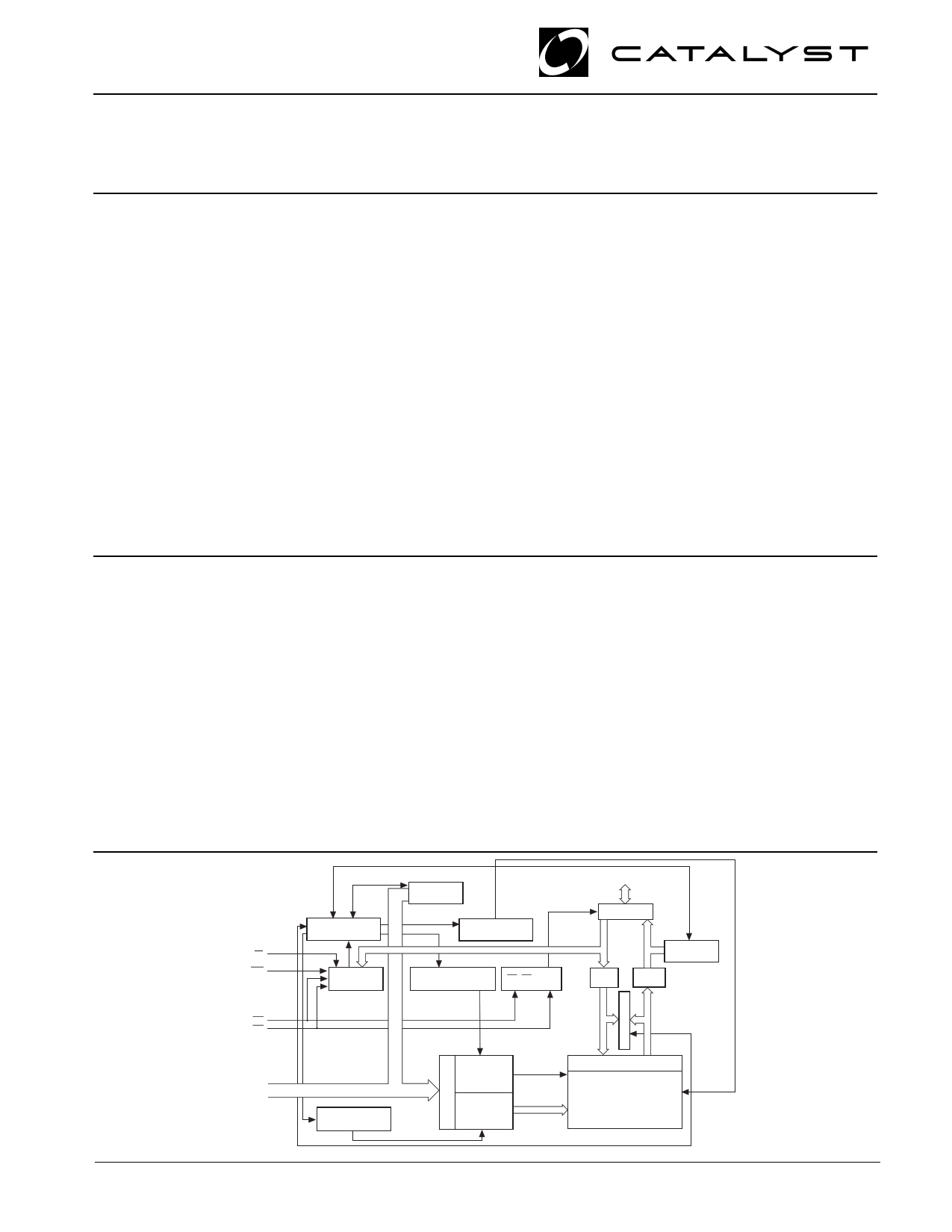
BLOCK DIAGRAM
RP
WE
WRITE STATE
MACHINE
COMMAND
REGISTER
ADDRESS
COUNTER
ERASE VOLTAGE
SWITCH
PROGRAM VOLTAGE
SWITCH
CE, OE LOGIC
I/O0–I/O7
I/O BUFFERS
DATA
LATCH
STATUS
REGISTER
SENSE
AMP
CE
OE
A0–A17
VOLTAGE VERIFY
SWITCH
Y-DECODER
X-DECODER
Y-GATING
16K-BYTE BOOT BLOCK
8K-BYTE PARAMETER BLOCK
8K-BYTE PARAMETER BLOCK
96K-BYTE MAIN BLOCK
128K-BYTE MAIN BLOCK
28F002 F01
© 1998 by Catalyst Semiconductor, Inc.
Characteristics subject to change without notice
1
Doc. No. 25072-00 2/98 F-1
1 page 
CAT28F002
SUPPLY CHARACTERISTICS
Symbol
VLKO
VCC
VPPL
VPPH
VHH
VPPLK
Parameter
VCC Erase/Write Lock Voltage
VCC Supply Voltage
VPP During Read Operations
VPP During Erase/Program
RP, OE Unlock Voltage
VPP Lock-Out Voltage
Limits
Min Max.
2.0
4.5 5.5
0 6.5
11.4 12.6
10.8 13.2
0 6.5
Unit
V
V
V
V
V
V
A.C. CHARACTERISTICS, Read Operation
VCC = +5V ±10%, unless otherwise specified
JEDEC Standard
Symbol Symbol
Parameter
tAVAV tRC Read Cycle Time
tELQV tCE CE Access Time
tAVQV
tACC Address Access Time
tGLQV tOE OE Access Time
- tOH Output Hold from Address OE/CE Change
tGLQX
tOLZ(1)(6) OE to Output in Low-Z
tELQX
tLZ(1)(6) CE to Output in Low-Z
tGHQZ
tDF(1)(2) OE High to Output High-Z
tEHQZ
tHZ(1)(2) CE High to Output High-Z
tPHQV
tPWH RP High to Output Delay
28F002-90 28F002-12 28F002-15
Min. Max. Min. Max. Min. Max. Unit
90 120 150 ns
90 120 150 ns
90 120 150 ns
40 40 40 ns
0 0 0 ns
0 0 0 ns
0 0 0 ns
30 30 30 ns
30 30 30 ns
300 300 300 ns
Figure 1. A.C. Testing Input/Output Waveform(3)(4)(5)
2.4 V
0.45 V
INPUT PULSE LEVELS
2.0 V
0.8 V
REFERENCE POINTS
5108 FHD F03
Figure 2. A.C. Testing Load Circuit (example)
1.3V
1N914
3.3K
DEVICE
UNDER
TEST
OUT
CL = 100 pF
Note:
CL INCLUDES JIG CAPACITANCE
(1) This parameter is tested initially and after a design or process change that affects the parameter.
(2) Output floating (High-Z) is defined as the state where the external data line is no longer driven by the output buffer.
(3) Input Rise and Fall Times (10% to 90%) < 10 ns.
(4) Input Pulse Levels = 0.45V and 2.4V.
(5) Input and Output Timing Reference = 0.8V and 2.0V.
(6) Low-Z is defined as the state where the external data may be driven by the output buffer but may not be valid.
5108 FHD F04
5 Doc. No. 25072-00 2/98 F-1
5 Page 
CAT28F002
IN-SYSTEM OPERATION
For on-board programming, the RP pin is the most
convenient means of altering the boot block. Before
issuing Program or Erase confirms commands, RP must
transition to VHH. Hold RP at this high voltage throughout
the program or erase interval (until after Status Register
confirm of successful completion). At this time, it can
return to VIH or VIL.
Figure 4 Byte Programming Flowchart
START
WRITE 40H,
BYTE ADDRESS
WRITE BYTE
ADDRESS/DATA
READ STATUS
REGISTER
SR.7 = 1?
YES
FULL STATUS
CHECK IF DESIRED
NO
BYTE PROGRAM
COMPLETED
FULL STATUS CHECK PROCEDURE
STATUS REGISTER DATA
READ (SEE ABOVE)
SR.3 = 0?
NO
VPP RANGE
ERROR
YES
SR.4 = 0?
NO BYTE PROGRAM
ERROR
YES
BYTE PROGRAM
SUCCESSFUL
Bus
Operation Command Comments
Write
Program
Setup
Data = 40H
Address = Bytes to be Programmed
Write
Program
Data to be programmed
Address = Byte to be Programmed
Read
Status Register Data.
Toggle OE or CE to update
Status Register
Check SR.7
Standby
1 = Ready, 0 = Busy
Repeat for subsequent bytes.
Full Status check can be done after each byte or after a sequence
of bytes.
Write FFH after the last byte programming operation to reset the
device to Read Array Mode.
Bus
Operation Command Comments
Standby
Check SR.3
1 = VPP Low Detect
Standby
Check SR.3
1 = Byte Program Error
SR.3 MUST be cleared, if set during a program attempt, before
further attempts are allowed by the Write State Machine.
SR.3 is only cleared by the Clear Status Register Command, in
case where multiple bytes are programmed before full status is
checked.
If error is detected, clear the Status Register before attempting retry
or other error recovery.
11 Doc. No. 25072-00 2/98 F-1
11 Page | ||
| Páginas | Total 16 Páginas | |
| PDF Descargar | [ Datasheet CAT28F002.PDF ] | |
Hoja de datos destacado
| Número de pieza | Descripción | Fabricantes |
| CAT28F001 | 1 Megabit CMOS Boot Block Flash Memory | Catalyst Semiconductor |
| CAT28F001 | 1 Megabit CMOS Boot Block Flash Memory | ON Semiconductor |
| CAT28F002 | 2 Megabit CMOS Boot Block Flash Memory | Catalyst Semiconductor |
| Número de pieza | Descripción | Fabricantes |
| SLA6805M | High Voltage 3 phase Motor Driver IC. |
Sanken |
| SDC1742 | 12- and 14-Bit Hybrid Synchro / Resolver-to-Digital Converters. |
Analog Devices |
|
DataSheet.es es una pagina web que funciona como un repositorio de manuales o hoja de datos de muchos de los productos más populares, |
| DataSheet.es | 2020 | Privacy Policy | Contacto | Buscar |