|
|
|
PDF CAT35C704 Data sheet ( Hoja de datos )
| Número de pieza | CAT35C704 | |
| Descripción | 4K-Bit Secure Access Serial E2PROM | |
| Fabricantes | Catalyst Semiconductor | |
| Logotipo | ||
Hay una vista previa y un enlace de descarga de CAT35C704 (archivo pdf) en la parte inferior de esta página. Total 14 Páginas | ||
|
No Preview Available !
Preliminary
CAT35C704
4K-Bit Secure Access Serial E2PROM
FEATURES
s Single 5V Supply
s Password READ/WRITE Protection: 1 to 8 Bytes
s Memory Pointer WRITE Protection
s Sequential READ Operation
s 256 x16 or 512 x 8 Selectable Serial Memory
s High Speed Synchronous Protocol
s Commercial, Industrial and Automotive
Temperature Ranges
DESCRIPTION
The CAT35C704 is a 4K-bit Serial E2PROM that safe-
guards stored data from unauthorized access by use of
a user selectable (1 to 8 byte) access code and a
movable memory pointer. Two operating modes provide
unprotected and password-protected operation allow-
ing the user to configure the device as anything from a
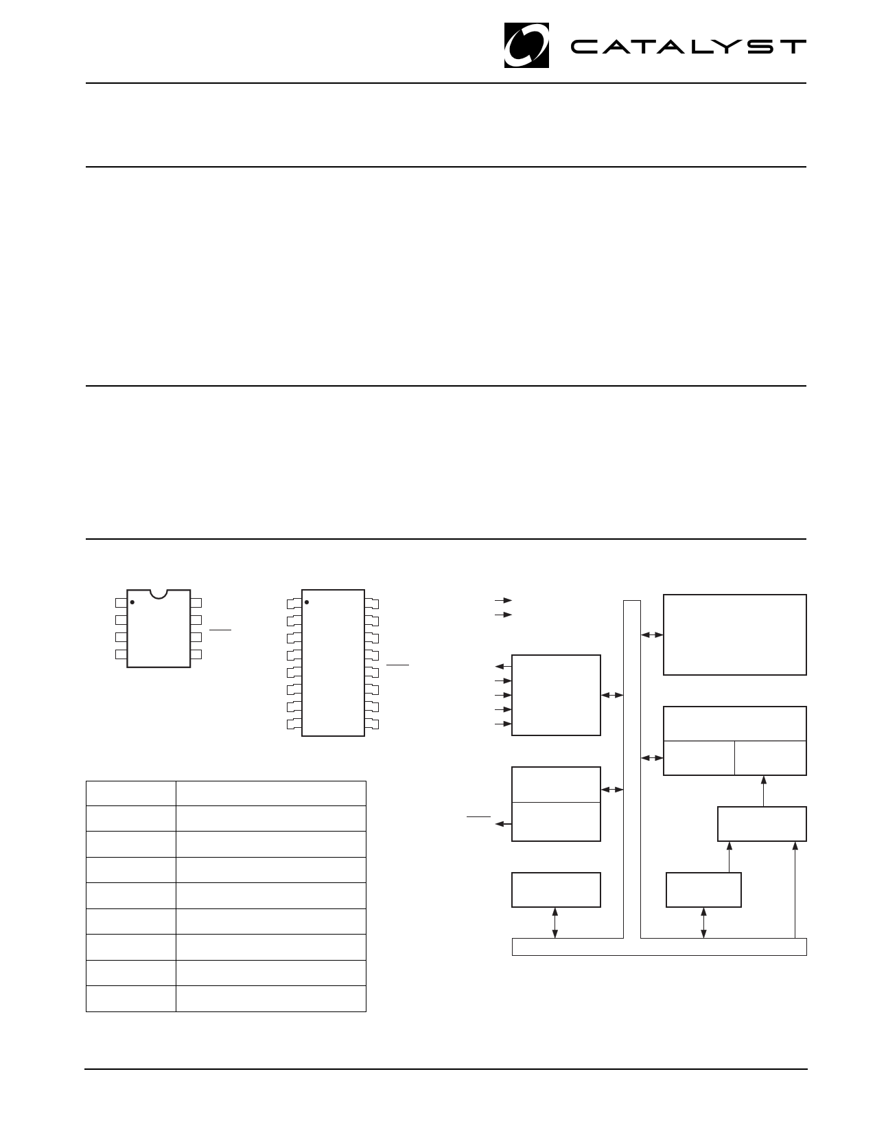
PIN CONFIGURATION
DIP Package (P)
SOIC Package (J)
CS 1
CLK 2
DI 3
DO 4
8 VCC
7 PE
NC 1 16 NC
NC 2 15 NC
6 ERR
CS 3 14 VCC
5 GND CLK 4 13 PE
DI 5 12 ERR
DO 6 11 GND
NC 7 10 NC
NC 8
9 NC
PIN FUNCTIONS
5074 FHD F01
Pin Name
Function
CS Chip Select
DO(1)
Serial Data Output
CLK Clock Input
DI(1)
Serial Data Input
PE Parity Enable
ERR
Error Indication Pin
VCC +5V Power Supply
GND
Ground
Note:
(1) DI, DO may be tied together to form a common I/O.
s Operating Frequency: DC–3MHz
s Low Power Consumption:
–Active: 3 mA
–Standby: 250 µA
s 100,000 Program/Erase Cycles
s 100 Year Data Retention
ROM to a fully protected no-access memory. The
CAT35C704 uses a unique serial-byte synchronous
communication protocol and has a Sequential Read
feature where data can be sequentially clocked out of
the memory array. The device is available in 8-pin DIP
or 16-pin SOIC packages.
BLOCK DIAGRAM
VCC
GND
DO
CLK
PE
CS
DI
SERIAL
COMMUNI-
CATION
BLOCK
ERR
INSTRUCTION
REGISTER
INSTRUCTION
DECODER
64-BIT ACCESS CODE
&
CONTROL BLOCK
4K-BIT EEPROM
ARRAY
R/W ADDRESS
BUFFER DECODER
ADDRESS
REGISTER
STATUS
REGISTER
MEMORY
POINTER
35C704 F02
© 1998 by Catalyst Semiconductor, Inc.
Characteristics subject to change without notice
1
Doc. No. 25045-00 2/98
1 page 
Preliminary
CAT35C704
READ SEQUENTIAL
To allow for convenient reading of blocks of contiguous
data, the device has a READ SEQUENTIAL instruction
which accepts a starting address of the block and
continuously outputs data of subsequent addresses
until the end of memory, or until Chip Select goes LOW.
The CAT35C704 communicates with external devices
via a synchronous serial communication protocol (SECS)
that has a maximum transmission rate of 3 MHz. The
data transmission may be a continuous stream of data
or it can be packed by pulsing Chip Select LOW in
between each packet of information. (Except for the
SEQUENTIAL READ instruction where Chip Select
must be held high).
PIN DESCRIPTIONS
CS
Chip Select is a TTL compatible input which, when set
HIGH, allows normal operation of the device. Any time
Chip Select is set LOW, it resets the device, terminating
all I/O communication, and puts the output in a high
impedance state. CS is used to reset the device if an
error condition exists or to put the device in a power-
down mode to minimize power consumption. It may also
be used to frame data transmission in applications
where the clock and data input have to be ignored from
time to time. Although CS resets the device, it does not
change the program/erase or the access-enable status,
nor does it terminate a programming cycle once it has
started. The program/erase and access-enable opera-
tions, once enabled, will remain enabled until specific
disabling instructions are sent or until power is removed.
Figure 3. Unprotected Mode(1)
ACCESS REGISTER:
ACCESS CODE LENGTH:
MEMORY POINTER:
x…x
0
a…a
POINTER
REGISTER
ADDRESS
IN MEMORY
READ/WRITE/ERASE
ACCESS
READ-ONLY
ACCESS
255 (x16)
511 (x8)
a…a
0
Figure 4. ERR Pin Timing
CS
CLK
ERR
HIGH-Z
Note:
(1) x = DON’T CARE; a = ADDRESS BIT.
tSV
tSV
5074 FHD F05
5074 FHD F06
5 Doc. No. 25045-00 2/98
5 Page 
Preliminary
CAT35C704
the following commands:
ERAL
ERAL
ERAL An ERAL will be executed
WRAL A WRAL will be executed
Both the ERAL and WRAL commands will program/
erase the entire array and will not be blocked by the
memory pointer.
THE PARITY BIT
The SECS protocol supports an even parity bit if the PE
pin of the device is set HIGH, otherwise, there is no
parity. If PE is set LOW and the incoming instruction
contains a parity bit, it may be interpreted as the start bit
of the next instruction. When PE is HIGH, the CAT35C704
expects a parity bit at the end of every incoming instruc-
tion packet. For example, the RSEQ instruction will look
like this:
1100 1011
A15…A8
A7…A0 P
The device then outputs data continuously until it reaches
the end of the memory. The last byte of data contains 9
bits. The ninth bit is the parity bit calculated over the
entire transmitted data packet. The RSEQ instruction
may be terminated at any time by bringing CS low; the
output will then go to high impedance.
SYSTEM ERRORS
Whenever an error occurs, be it an instruction error
(unknown instruction), or parity error (perhaps caused
by transmission error), the device will stop its operation.
To return to normal operation, the device must be reset
by pulsing CS LOW and then set back to HIGH. Reset-
ting the device will not affect the ENAC, EWEN and
ENBSY status. The error may be determined by entering
the READ STATUS REGISTER (RSR) instruction
immediatly following the reset. The status output is an 8
bit word with the first three bits being 101. This three bit
pattern indicates that the device is functioning normally.
The fourth bit is “1” if a parity error occurred. The fifth bit
is a “1” if an instruction error occurred. The sixth bit is a
“1” if the device is in a program/erase cycle. The last two
bits are reserved for future use.
The reason for the “101” pattern is to distinguish be-
tween an error conditon (DO tri-stated) and a device
busy status. If an error condition exists, it will not respond
to any input instruction from DI. However, if the device is
in a program/erase cycle, it responds to the RSR instruc-
tion by outputting “101 00100”. If RSR is executed at the
end of a program/erase cycle, the output will be “101000
00”.
10 1 X X X X X
Figure 13. Next Instruction Timing(1)
CS
PARITY
ERROR
INSTRUCTION RDY/BUSY
ERROR
STATUS
FUTURE USE
5074 FHD F09
CLK
tEW
tSV
DI
NEXT INSTRUCTION
HIGH-Z
DO
OP CODE
READY
tHZ
HIGH-Z
BUSY
5074 FHD F16
Note:
(1) DO will be high impedance after the last instruction bit has been clocked in, unless the instruction is RSR or RMPR, in which case, DO will
become active.
11 Doc. No. 25045-00 2/98
11 Page | ||
| Páginas | Total 14 Páginas | |
| PDF Descargar | [ Datasheet CAT35C704.PDF ] | |
Hoja de datos destacado
| Número de pieza | Descripción | Fabricantes |
| CAT35C704 | 4K-Bit Secure Access Serial E2PROM | Catalyst Semiconductor |
| Número de pieza | Descripción | Fabricantes |
| SLA6805M | High Voltage 3 phase Motor Driver IC. |
Sanken |
| SDC1742 | 12- and 14-Bit Hybrid Synchro / Resolver-to-Digital Converters. |
Analog Devices |
|
DataSheet.es es una pagina web que funciona como un repositorio de manuales o hoja de datos de muchos de los productos más populares, |
| DataSheet.es | 2020 | Privacy Policy | Contacto | Buscar |