|
|
PDF S-19311 Data sheet ( Hoja de datos )
| Número de pieza | S-19311 | |
| Descripción | HIGH-WITHSTAND VOLTAGE CMOS VOLTAGE REGULATOR | |
| Fabricantes | Seiko | |
| Logotipo |  |
|
Hay una vista previa y un enlace de descarga de S-19311 (archivo pdf) en la parte inferior de esta página. Total 30 Páginas | ||
|
No Preview Available !
S-19311 Series
FOR AUTOMOTIVE 125°C OPERATION HIGH-WITHSTAND VOLTAGE
www.sii-ic.com
CMOS VOLTAGE REGULATOR WITH RESET FUNCTION
© SII Semiconductor Corporation, 2015-2017
Rev.1.1_00
The S-19311 Series, developed by using high-withstand voltage CMOS technology, is a positive voltage regulator with the
reset function, which has high-withstand voltage and high-accuracy output voltage. This IC has a built-in low on-resistance
output transistor which provides a small dropout voltage and a large output current. Also, a built-in overcurrent protection
circuit to limit overcurrent of the output transistor and a built-in thermal shutdown circuit to limit heat are included.
High heat radiation TO-252-5S(A) and HSOP-8A packages enable high-density mounting.
Caution This product can be used in vehicle equipment and in-vehicle equipment. Before using the product in
the purpose, contact to SII Semiconductor Corporation is indispensable.
Features
Regulator block
• Output voltage:
• Input voltage:
• Output voltage accuracy:
• Dropout voltage:
• Output current:
• Input and output capacitors:
• Ripple rejection:
• Built-in overcurrent protection circuit:
• Built-in thermal shutdown circuit:
3.0 V to 5.3 V, selectable in 0.1 V step
4.0 V to 36.0 V
±2.0% (Tj = −40°C to +150°C)
120 mV typ. (5.0 V output product, IOUT = 100 mA)
Possible to output 200 mA (VIN = VOUT(S) + 1.0 V)*1
A ceramic capacitor of 2.2 μF or more can be used.
70 dB typ. (f = 100 Hz)
Limits overcurrent of output transistor.
Detection temperature 170°C typ.
Detector block
• Detection voltage:
• Detection voltage accuracy:
• Hysteresis width:
• Release delay time:
• Output form:
2.6 V to 5.0 V, selectable in 0.1 V step
±100 mV (Tj = −40°C to +150°C)
0.12 V min.
18 ms typ. (CDLY = 47 nF)
Nch open-drain output (Built-in pull-up resistor)
Overall
• Current consumption:
• Operation temperature range:
• Lead-free (Sn 100%), halogen-free
• Withstand 45 V load dump
• AEC-Q100 qualified*2
During operation: 60 μA typ., 95 μA max. (Tj = −40°C to +150°C)
Ta = −40°C to +125°C
*1. Please make sure that the loss of the IC will not exceed the power dissipation when the output current is large.
*2. Contact our sales office for details.
Applications
• Constant-voltage power supply and reset circuit for automotive electric component
• For automotive use (engine, transmission, suspension, ABS, related-devices for EV / HEV / PHEV, etc.)
Packages
• TO-252-5S(A)
• HSOP-8A
1
1 page 
FOR AUTOMOTIVE 125°C OPERATION HIGH-WITHSTAND VOLTAGE CMOS VOLTAGE REGULATOR WITH RESET FUNCTION
Rev.1.1_00
S-19311 Series
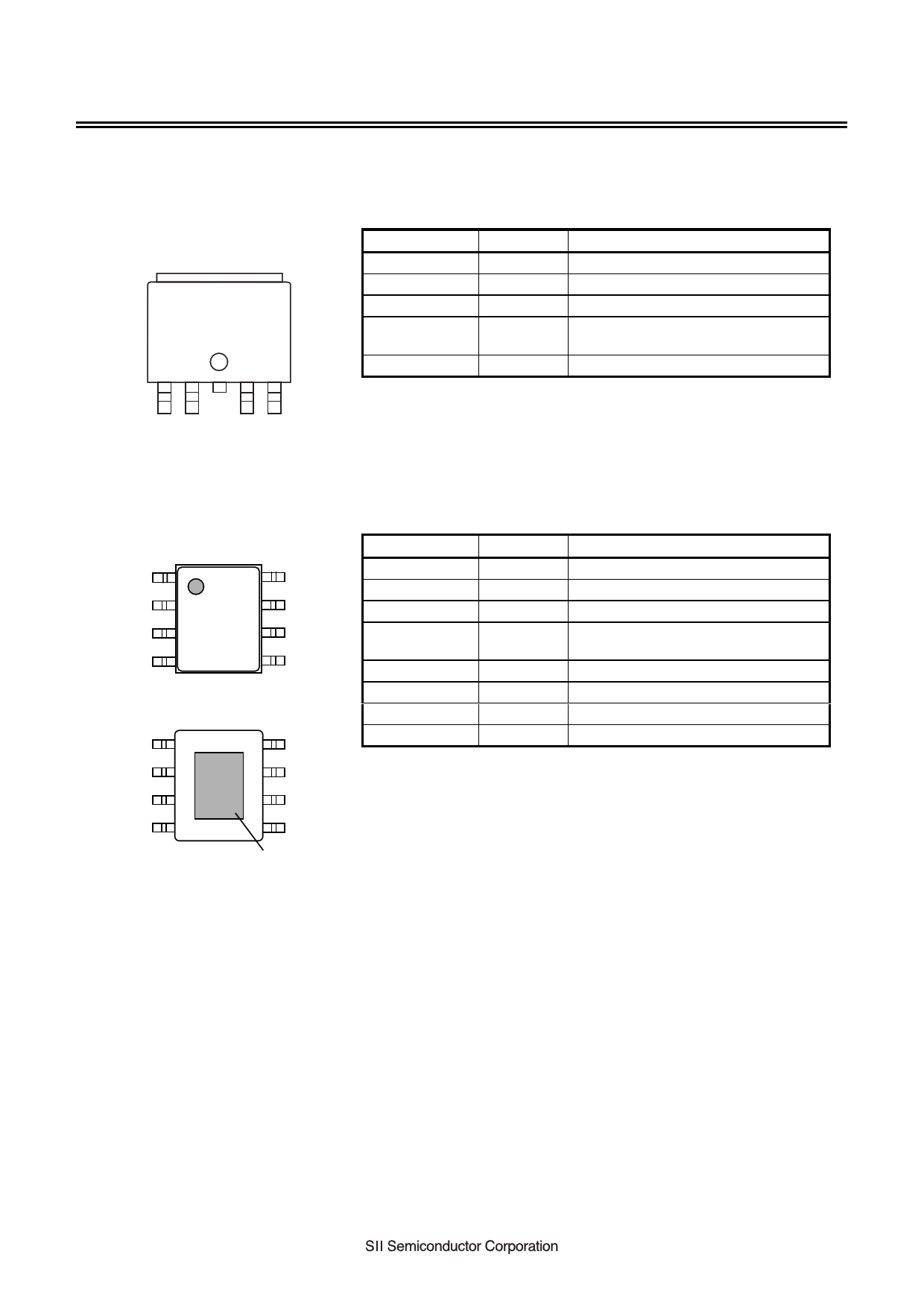
Pin Configurations
1. TO-252-5S(A)
Top view
3
Pin No.
1
2
3
4
5
Symbol
VIN
VOUT
VSS
DLY
RO
Table 3
Description
Voltage input pin (Regulator block)
Voltage output pin (Regulator block)
GND pin
Connection pin for delay time
adjustment capacitor
Reset output pin
12
45
Figure 2
2. HSOP-8A
Top view
1
2
3
4
8
7
6
5
Bottom view
81
72
63
54
*1
Table 4
Pin No.
Symbol
Description
1
VOUT
Voltage output pin (Regulator block)
2 NC*1 No connection
3 VSS GND pin
4
DLY
Connection pin for delay time
adjustment capacitor
5 RO
Reset output pin
6 NC*1 No connection
7 NC*1 No connection
8 VIN
Voltage input pin (Regulator block)
*1. The NC pin is electrically open.
The NC pin can be connected to the VDD pin or the VSS pin.
*1. Connect the heat sink of backside
at shadowed area to the board,
and set electric potential open or
GND.
However, do not use it as the
function of electrode.
Figure 3
5
5 Page 
FOR AUTOMOTIVE 125°C OPERATION HIGH-WITHSTAND VOLTAGE CMOS VOLTAGE REGULATOR WITH RESET FUNCTION
Rev.1.1_00
S-19311 Series
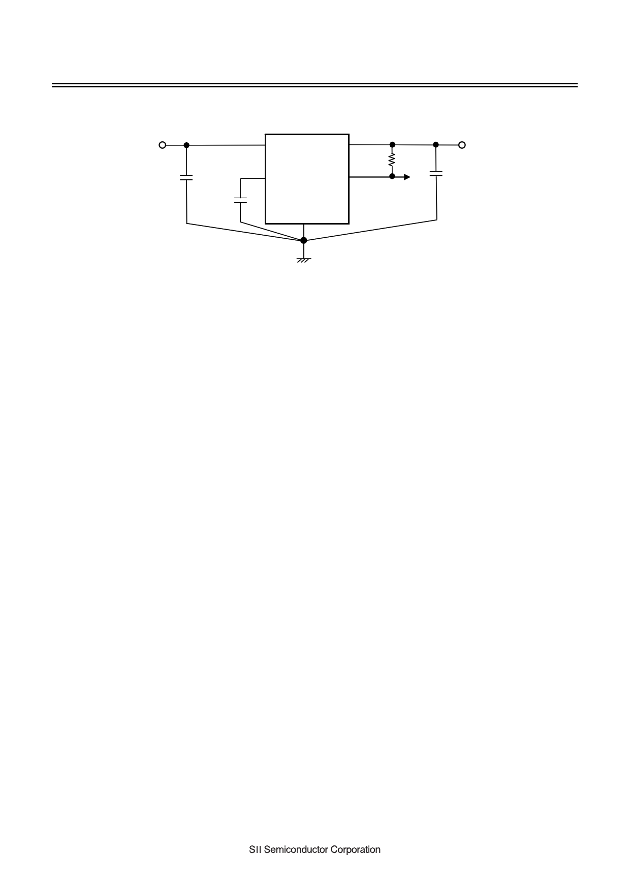
Standard Circuit
Input
CIN*1
CDLY*3
VIN
DLY
VOUT
RO
VSS
Rext*4
Output
CL*2
Single GND GND
Figure 12
*1. CIN is a capacitor for stabilizing the input.
*2. CL is a capacitor for stabilizing the output. A ceramic capacitor of 2.2 μF or more can be used.
*3. CDLY is the delay time adjustment capacitor.
*4. Rext is the external pull-up resistor for the reset output pin.
Connection of the external pull-up resistor is not absolutely essential since the S-19311 Series
has a built-in pull-up resistor.
Caution The above connection diagram and constants will not guarantee successful operation. Perform
thorough evaluation using an actual application to set the constants.
11
11 Page | ||
| Páginas | Total 30 Páginas | |
| PDF Descargar | [ Datasheet S-19311.PDF ] | |
Hoja de datos destacado
| Número de pieza | Descripción | Fabricantes |
| S-19311 | HIGH-WITHSTAND VOLTAGE CMOS VOLTAGE REGULATOR | Seiko |
| Número de pieza | Descripción | Fabricantes |
| SLA6805M | High Voltage 3 phase Motor Driver IC. |
Sanken |
| SDC1742 | 12- and 14-Bit Hybrid Synchro / Resolver-to-Digital Converters. |
Analog Devices |
|
DataSheet.es es una pagina web que funciona como un repositorio de manuales o hoja de datos de muchos de los productos más populares, |
| DataSheet.es | 2020 | Privacy Policy | Contacto | Buscar |
