|
|
|
PDF M28C64 Data sheet ( Hoja de datos )
| Número de pieza | M28C64 | |
| Descripción | 64 Kbit (8K x 8) Parallel EEPROM | |
| Fabricantes | STMicroelectronics | |
| Logotipo | ||
Hay una vista previa y un enlace de descarga de M28C64 (archivo pdf) en la parte inferior de esta página. Total 24 Páginas | ||
|
No Preview Available !
M28C64
64 Kbit (8K x 8) Parallel EEPROM
With Software Data Protection
NOT FOR NEW DESIGN
s Fast Access Time:
– 90 ns at VCC=5 V for M28C64 and M28C64-A
– 120 ns at VCC=3 V for M28C64-xxW
s Single Supply Voltage:
– 4.5 V to 5.5 V for M28C64 and M28C64-A
– 2.7 V to 3.6 V for M28C64-xxW
s Low Power Consumption
s Fast BYTE and PAGE WRITE (up to 64 Bytes)
– 1 ms at VCC=4.5 V for M28C64-A
– 3 ms at VCC=4.5 V for M28C64
– 5 ms at VCC=2.7 V for M28C64-xxW
s Enhanced Write Detection and Monitoring:
– Ready/Busy Open Drain Output
– Data Polling
– Toggle Bit
– Page Load Timer Status
s JEDEC Approved Bytewide Pin-Out
s Software Data Protection
s 100000 Erase/Write Cycles (minimum)
s Data Retention (minimum):
– 40 Years for M28C64 and M28C64-xxW
– 10 Years for M28C64-A
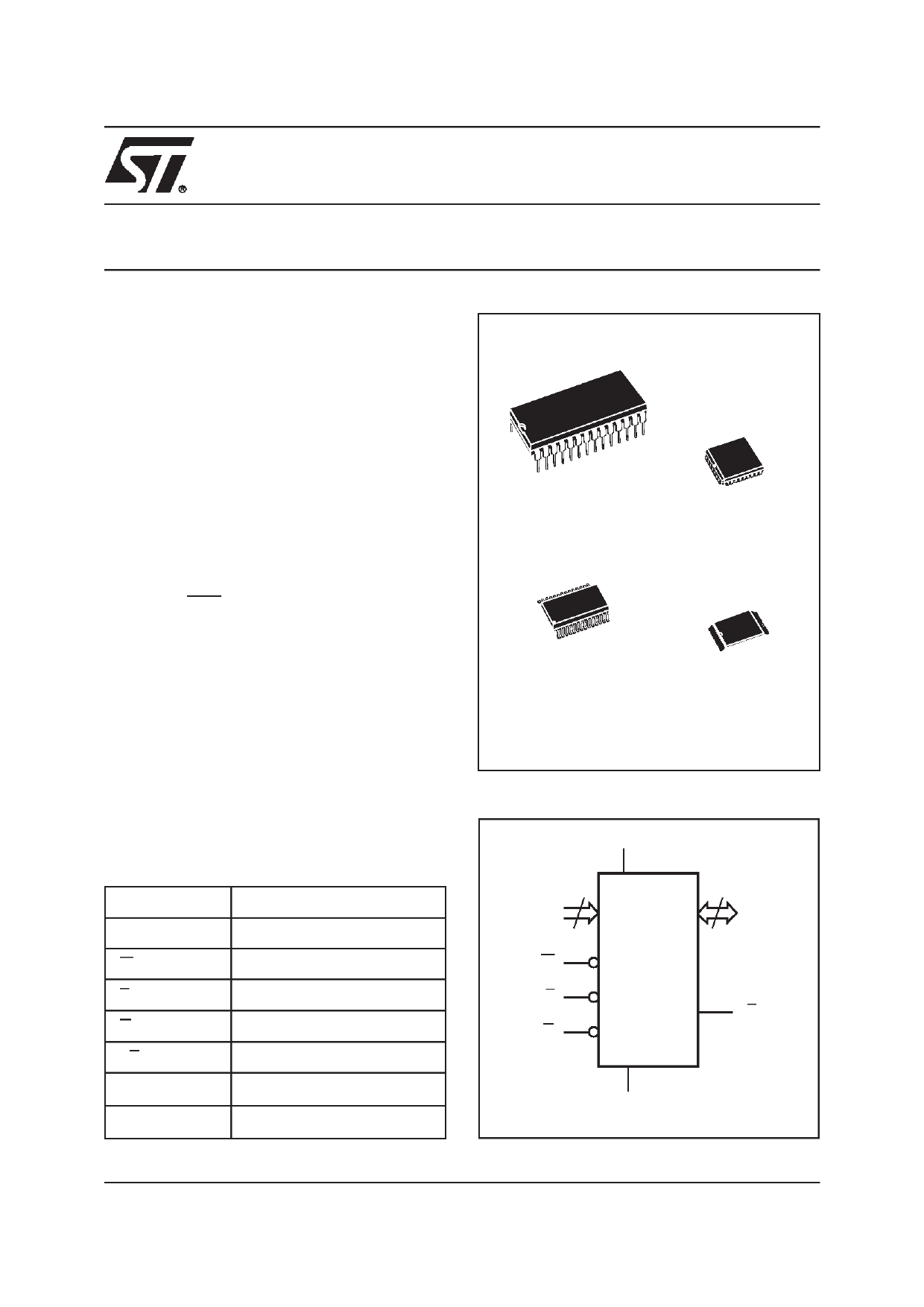
28
1
PDIP28 (BS)
28
1
SO28 (MS)
300 mil width
Figure 1. Logic Diagram
VCC
PLCC32 (KA)
TSOP28 (NS)
8 x 13.4 mm
Table 1. Signal Names
A0-A12
Address Input
DQ0-DQ7
Data Input / Output
W Write Enable
E Chip Enable
G Output Enable
RB Ready / Busy
VCC
Supply Voltage
VSS Ground
13
A0-A12
8
DQ0-DQ7
W M28C64
E
RB
G
VSS
AI01350C
April 2001
This is information on a product still in production but not recommended for new designs.
1/24
1 page 
M28C64
Read
The device is accessed like a static RAM. When E
and G are low, and W is high, the contents of the
addressed location are presented on the I/O pins.
Otherwise, when either G or E is high, the I/O pins
revert to their high impedance state.
Write
Write operations are initiated when both W and E
are low and G is high. The device supports both
W-controlled and E-controlled write cycles (as
shown in Figure 11 and Figure 12). The address is
latched during the falling edge of W or E (which
ever occurs later) and the data is latched on the
rising edge of W or E (which ever occurs first).
After a delay, tWLQ5H, that cannot be shorter than
the value specified in Table 10A to Table 10C, the
internal write cycle starts. It continues, under
internal timing control, until the write operation is
complete. The commencement of this period can
be detected by reading the Page Load Timer
Status on DQ5. The end of the cycle can be
detected by reading the status of the Data Polling
and the Toggle Bit functions on DQ7 and DQ6.
Page Write
The Page Write mode allows up to 64 bytes to be
written on a single page in a single go. This is
achieved through a series of successive Write
operations, no two of which are separated by more
than the tWLQ5H value (as specified in Table 10A
to Table 10C).
All bytes must be located on the same page
address (A12-A6 must be the same for all bytes).
The internal write cycle can start at any instant
after tWLQ5H. Once initiated, the write operation is
internally timed, and continues, uninterrupted,
until completion.
As with the single byte Write operation, described
above, the DQ5, DQ6 and DQ7 lines can be used
to detect the beginning and end of the internally
controlled phase of the Page Write cycle.
Software Data Protection (SDP)
The device offers a software-controlled write-
protection mechanism that allows the user to
inhibit all write operations to the device. This can
be useful for protecting the memory from
inadvertent write cycles that may occur during
periods of instability (uncontrolled bus conditions
when excessive noise is detected, or when power
supply levels are outside their specified values).
By default, the device is shipped in the
“unprotected” state: the memory contents can be
freely changed by the user. Once the Software
Data Protection Mode is enabled, all write
commands are ignored, and have no effect on the
memory contents.
The device remains in this mode until a valid
Software Data Protection disable sequence is
received. The device reverts to its “unprotected”
state.
The status of the Software Data Protection
(enabled or disabled) is represented by a non-
Figure 4. Software Data Protection Enable Algorithm and Memory Write
Page Write
Timing
(see note 1)
Write AAh in
Address 1555h
Write 55h in
Address 0AAAh
Write A0h in
Address 1555h
Page Write
Timing
(see note 1)
Write AAh in
Address 1555h
Write 55h in
Address 0AAAh
Write A0h in
Address 1555h
SDP is set
Physical
Page Write
Instruction
Page Write
(1 up to 64 bytes)
Write
is enabled
SDP Enable Algorithm
Write to Memory
When SDP is SET
AI01356C
Note: 1. The most significant address bits (A12 to A6) differ during these specific Page Write operations.
5/24
5 Page 
M28C64
Table 9C. Read Mode AC Characteristics for M28C64-xxW (3V range)
(TA = 0 to 70 °C or –40 to 85 °C; VCC = 2.7 to 3.6 V)
Symbol Alt.
Parameter
Test
Condit
ion
-12
Min Max
M28C64-xxW
-15 -20 -25
Min Max Min Max Min Max
-30
Min Max
Unit
tAVQV
tACC
Address Valid to
Output Valid
E =VIL,
G = VIL
120
150
200
250
300 ns
tELQV
tCE
Chip Enable Low to
Output Valid
G = VIL
120
150
200
250
300 ns
tGLQV
tOE
Output Enable Low
to Output Valid
E = VIL
80
80 100 150 150 ns
tEHQZ1
tDF
Chip Enable High to
Output Hi-Z
G = VIL
0
45
0
50
0
55
0
60
0
60 ns
tGHQZ1
tDF
Output Enable High
to Output Hi-Z
E = VIL
0
45
0
50
0
55
0
60
0
60 ns
tAXQX
tOH
Address Transition
to Output Transition
E =VIL,
G = VIL
0
0
0
0
0 ns
Note: 1. Output Hi-Z is defined as the point at which data is no longer driven.
Figure 10. Read Mode AC Waveforms (with Write Enable, W, high)
A0-A12
E
G
DQ0-DQ7
Note: 1. Write Enable (W) = VIH
tAVQV
VALID
tAXQX
tGLQV
tEHQZ
tELQV
DATA OUT
tGHQZ
Hi-Z
AI00749B
11/24
11 Page | ||
| Páginas | Total 24 Páginas | |
| PDF Descargar | [ Datasheet M28C64.PDF ] | |
Hoja de datos destacado
| Número de pieza | Descripción | Fabricantes |
| M28C64 | 64 Kbit (8K x 8) Parallel EEPROM | STMicroelectronics |
| M28C64C | 64 Kbit (8Kb x8) Parallel EEPROM | STMicroelectronics |
| M28C64X | 64 Kbit (8Kb x8) Parallel EEPROM | STMicroelectronics |
| Número de pieza | Descripción | Fabricantes |
| SLA6805M | High Voltage 3 phase Motor Driver IC. |
Sanken |
| SDC1742 | 12- and 14-Bit Hybrid Synchro / Resolver-to-Digital Converters. |
Analog Devices |
|
DataSheet.es es una pagina web que funciona como un repositorio de manuales o hoja de datos de muchos de los productos más populares, |
| DataSheet.es | 2020 | Privacy Policy | Contacto | Buscar |