|
|
PDF HM5225405BLTT-75 Data sheet ( Hoja de datos )
| Número de pieza | HM5225405BLTT-75 | |
| Descripción | 256M LVTTL interface SDRAM 133 MHz/100 MHz 4-Mword 16-bit 4-bank/8-Mword 8-bit 4-bank /16-Mword 4-bit 4-bank PC/133/ PC/100 SDRAM | |
| Fabricantes | Elpida Memory | |
| Logotipo |  |
|
Hay una vista previa y un enlace de descarga de HM5225405BLTT-75 (archivo pdf) en la parte inferior de esta página. Total 63 Páginas | ||
|
No Preview Available !
HM5225165B-75/A6/B6
HM5225805B-75/A6/B6
HM5225405B-75/A6/B6
256M LVTTL interface SDRAM
133 MHz/100 MHz
4-Mword × 16-bit × 4-bank/8-Mword × 8-bit × 4-bank
/16-Mword × 4-bit × 4-bank
PC/133, PC/100 SDRAM
E0082H10 (1st edition)
(Previous ADE-203-1073B (Z))
Jan. 31, 2001
Description
The HM5225165B is a 256-Mbit SDRAM organized as 4194304-word × 16-bit × 4 bank. The HM5225805B
is a 256-Mbit SDRAM organized as 8388608-word × 8-bit × 4 bank. The HM5225405B is a 256-Mbit
SDRAM organized as 16777216-word × 4-bit × 4 bank. All inputs and outputs are referred to the rising edge
of the clock input. It is packaged in standard 54-pin plastic TSOP II.
Features
• 3.3 V power supply
• Clock frequency: 133 MHz/100 MHz (max)
• LVTTL interface
• Single pulsed RAS
• 4 banks can operate simultaneously and independently
• Burst read/write operation and burst read/single write operation capability
• Programmable burst length: 1/2/4/8
• 2 variations of burst sequence
Sequential (BL = 1/2/4/8)
Interleave (BL = 1/2/4/8)
• Programmable CAS latency: 2/3
Elpida Memory, Inc. is a joint venture DRAM company of NEC Corporation and Hitachi, Ltd.
1 page 
HM5225165B/HM5225805B/HM5225405B-75/A6/B6
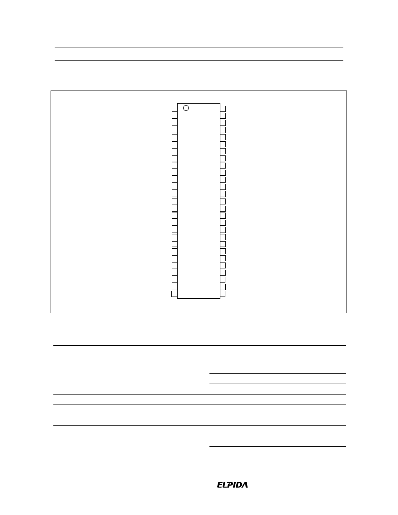
Pin Arrangement (HM5225405B)
VCC
NC
VCCQ
NC
DQ0
VSSQ
NC
NC
VCCQ
NC
DQ1
VSSQ
NC
VCC
NC
WE
CAS
RAS
CS
BA0
BA1
A10
A0
A1
A2
A3
VCC
54-pin TSOP
1 54
2 53
3 52
4 51
5 50
6 49
7 48
8 47
9 46
10 45
11 44
12 43
13 42
14 41
15 40
16 39
17 38
18 37
19 36
20 35
21 34
22 33
23 32
24 31
25 30
26 29
27 28
(Top view)
VSS
NC
VSSQ
NC
DQ3
VCCQ
NC
NC
VSSQ
NC
DQ2
VCCQ
NC
VSS
NC
DQM
CLK
CKE
A12
A11
A9
A8
A7
A6
A5
A4
VSS
Pin Description
Pin name
A0 to A12,
BA0, BA1
DQ0 to DQ3
CS
RAS
CAS
Function
Address input
Pin name
WE
Row address
A0 to A12
Column address
A0 to A9, A11
Bank select address BA0/BA1 (BS)
Data-input/output
Chip select
Row address strobe command
Column address strobe command
DQM
CLK
CKE
VCC
VSS
VCCQ
VSSQ
NC
Function
Write enable
Input/output mask
Clock input
Clock enable
Power for internal circuit
Ground for internal circuit
Power for DQ circuit
Ground for DQ circuit
No connection
Data Sheet E0082H10
5
5 Page 
HM5225165B/HM5225805B/HM5225405B-75/A6/B6
Column address strobe and write command [WRIT]: This command starts a write operation. When the
burst write mode is selected, the column address (AY0 to AY8; HM5225165B, AY0 to AY9; HM5225805B,
AY0 to AY9, AY11; HM5225405B) and the bank select address (BA0/BA1) become the burst write start
address. When the single write mode is selected, data is only written to the location specified by the column
address (AY0 to AY8; HM5225165B, AY0 to AY9; HM5225805B, AY0 to AY9, AY11; HM5225405B) and
the bank select address (BA0/BA1).
Write with auto-precharge [WRIT A]: This command automatically performs a precharge operation after a
burst write with a length of 1, 2, 4 or 8, or after a single write operation.
Row address strobe and bank activate [ACTV]: This command activates the bank that is selected by
BA0/BA1 (BS) and determines the row address (AX0 to AX12). When BA0 and BA1 are Low, bank 0 is
activated. When BA0 is Low and BA1 is High, bank 1 is activated. When BA0 is High and BA1 is Low,
bank 2 is activated. When BA0 and BA1 are High, bank 3 is activated.
Precharge selected bank [PRE]: This command starts precharge operation for the bank selected by
BA0/BA1. If BA0 and BA1 are Low, bank 0 is selected. If BA0 is Low and BA1 is High, bank 1 is selected.
If BA0 is High and BA1 is Low, bank 2 is selected. If BA0 and BA1 are High, bank 3 is selected.
Precharge all banks [PALL]: This command starts a precharge operation for all banks.
Refresh [REF/SELF]: This command starts the refresh operation. There are two types of refresh operation,
the one is auto-refresh, and the other is self-refresh. For details, refer to the CKE truth table section.
Mode register set [MRS]: The SDRAM has a mode register that defines how it operates. The mode register
is specified by the address pins (A0 to BA0 and BA1) at the mode register set cycle. For details, refer to the
mode register configuration. After power on, the contents of the mode register are undefined, execute the
mode register set command to set up the mode register.
Data Sheet E0082H10
11
11 Page | ||
| Páginas | Total 63 Páginas | |
| PDF Descargar | [ Datasheet HM5225405BLTT-75.PDF ] | |
Hoja de datos destacado
| Número de pieza | Descripción | Fabricantes |
| HM5225405BLTT-75 | 256M LVTTL interface SDRAM 133 MHz/100 MHz 4-Mword 16-bit 4-bank/8-Mword 8-bit 4-bank /16-Mword 4-bit 4-bank PC/133/ PC/100 SDRAM | Elpida Memory |
| Número de pieza | Descripción | Fabricantes |
| SLA6805M | High Voltage 3 phase Motor Driver IC. |
Sanken |
| SDC1742 | 12- and 14-Bit Hybrid Synchro / Resolver-to-Digital Converters. |
Analog Devices |
|
DataSheet.es es una pagina web que funciona como un repositorio de manuales o hoja de datos de muchos de los productos más populares, |
| DataSheet.es | 2020 | Privacy Policy | Contacto | Buscar |
