|
|
|
PDF 74ACTQ652MTC Data sheet ( Hoja de datos )
| Número de pieza | 74ACTQ652MTC | |
| Descripción | Quiet Series Transceiver/Register | |
| Fabricantes | Fairchild Semiconductor | |
| Logotipo | ||
Hay una vista previa y un enlace de descarga de 74ACTQ652MTC (archivo pdf) en la parte inferior de esta página. Total 9 Páginas | ||
|
No Preview Available !
June 1991
Revised November 1999
74ACTQ652
Quiet Series Transceiver/Register
General Description
The ACTQ652 consists of bus transceiver circuits with D-
type flip-flops, and control circuitry arranged for multiplexed
transmission of data directly from the input bus or from
internal registers. Data on the A or B bus will be clocked
into the registers as the appropriate clock pin goes to the
HIGH logic level. Output Enable pins (OEAB, OEBA) are
provided to control the transceiver function.
The ACTQ652 utilizes Fairchild FACT Quiet Series tech-
nology to guarantee quiet output switching and improved
dynamic threshold performance. FACT Quiet Series fea-
tures GTO output control and undershoot corrector in
addition to split ground bus for superior performance.
Features
s Guaranteed simultaneous switching noise level and
dynamic threshold performance
s Guaranteed pin-to-pin skew AC performance
s Independent registers for A and B buses
s Multiplexed real-time and stored data
s Outputs source/sink 24 mA
s TTL-compatible inputs
Ordering Code:
Order Number Package Number
Package Description
74ACTQ652SC
M24B
24-Lead Small Outline Integrated Circuit (SOIC), JEDEC MS-013, 0.300” Wide Body
74ACTQ652MTC
MTC24
24-Lead Thin Shrink Small Outline Package (TSSOP), JEDEC MO-153, 4.4mm Wide
74ACTQ652SPC
N24C
24-Lead Plastic Dual-In-Line Package (PDIP), JEDEC MS-100, 0.300” Wide
Device also available in Tape and Reel. Specify by appending suffix letter “X” to the ordering code.
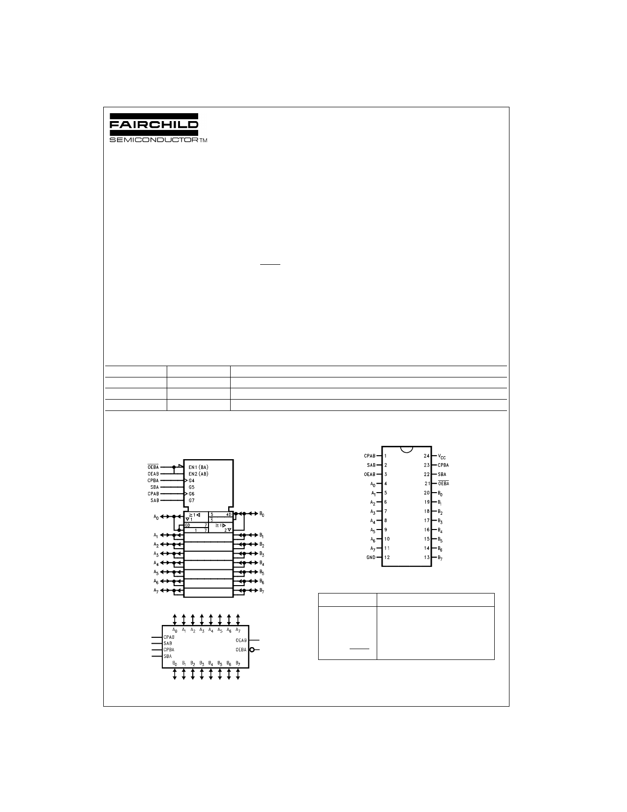
Logic Symbols
Connection Diagram
IEEE/IEC
Pin Descriptions
Pin Names
A0–A7, B0–B7
CPAB, CPBA
SAB, SBA
OEAB, OEBA
Description
A and B Inputs/3-STATE Outputs
Clock Inputs
Select Inputs
Output Enable Inputs
FACT, Quiet Series, FACT Quiet Series and GTO are trademarks of Fairchild Semiconductor Corporation.
© 1999 Fairchild Semiconductor Corporation DS010933
www.fairchildsemi.com
1 page 
DC Electrical Characteristics (Continued)
Symbol
Parameter
VCC
TA = +25°C
TA = −40°C to +85°C
Units
(V) Typ
Guaranteed Limits
Conditions
VILD
Maximum LOW Level
Dynamic Input Voltage
5.0 1.2 0.8
V (Note 5)(Note 7)
Note 3: All outputs loaded; thresholds on input associated with output under test.
Note 4: Maximum test duration 2.0 ms, one output loaded at a time.
Note 5: PDIP package.
Note 6: Max number of outputs defined as (n). Data inputs are driven 0V to 3V. One output @ GND.
Note 7: Max number of data inputs (n) switching. (n − 1) inputs switching 0V to 3V (ACTQ). Input-under-test switching: 3V to threshold (VILD),
0V to threshold (VIHD), f = 1 MHz.
AC Electrical Characteristics
VCC
TA = +25°C
TA = −40°C to +85°C
Symbol
Parameter
(V) CL = 50 pF
CL = 50 pF
Units
(Note 8)
Min
Typ
Max
Min
Max
fMAX
tPLH
tPHL
tPLH
tPHL
tPLH
tPHL
tPZH
tPZL
tPHZ
tPLZ
tPZH
tPZL
tPHZ
tPLZ
ts(H)
ts(L)
th(H)
th(L)
tw(H)
tw(L)
tOSHL
tOSLH
Maximum Clock Frequency
Propagation Delay
Clock to Bus
Propagation Delay
Bus to Bus
Propagation Delay
SBA or SAB to A or B
Enable Time
OEBA to A (Note 8)
Disable Time
OEBA to A (Note 8)
Enable Time
OEAB to B
Disable Time
OEAB to B
Setup Time, HIGH or
LOW, Bus to Clock
Hold Time, HIGH or
LOW, Bus to Clock
Clock Pulse Width
HIGH or LOW
Output to Output Skew (Note 9)
A to B, B to A or
Clock to Output
5.0 MHz
5.0 2.0 7.0 9.5 2.0 10.0 ns
5.0 2.0 6.5 9.0 2.0 9.5 ns
5.0 2.5 6.5 10.0 2.5 10.5 ns
5.0 2.0 7.0 10.5 2.0 11.0
5.0 1.0 5.0 8.0 1.0 8.5 ns
5.0 2.0 7.0 10.5 2.0 11.0
5.0 1.0 5.0 8.0 1.0 8.5 ns
5.0 3.0
3.0 ns
5.0 1.5
1.5 ns
5.0 4.0
4.0 ns
5.0 0.5 1.0 1.0 ns
Note 8: Voltage Range 5.0 is 5.0V ± 0.5V.
Note 9: Skew is defined as the absolute value of the difference between the actual propagation delay for any separate outputs of the same device. The spec-
ification applies to any output switching in the same direction, either HIGH-to-LOW (TOSHL) or LOW-to-HIGH (TOSLH). Parameter guaranteed by design.
Capacitance
Symbol
CIN
CPD
Parameter
Input Capacitance
Power Dissipation Capacitance
Typ Units
Conditions
4.5 pF VCC = 5.0V
54 pF VCC = 5.0V
5 www.fairchildsemi.com
5 Page | ||
| Páginas | Total 9 Páginas | |
| PDF Descargar | [ Datasheet 74ACTQ652MTC.PDF ] | |
Hoja de datos destacado
| Número de pieza | Descripción | Fabricantes |
| 74ACTQ652MTC | Quiet Series Transceiver/Register | Fairchild Semiconductor |
| Número de pieza | Descripción | Fabricantes |
| SLA6805M | High Voltage 3 phase Motor Driver IC. |
Sanken |
| SDC1742 | 12- and 14-Bit Hybrid Synchro / Resolver-to-Digital Converters. |
Analog Devices |
|
DataSheet.es es una pagina web que funciona como un repositorio de manuales o hoja de datos de muchos de los productos más populares, |
| DataSheet.es | 2020 | Privacy Policy | Contacto | Buscar |