|
|
|
PDF 74ACT16240MTD Data sheet ( Hoja de datos )
| Número de pieza | 74ACT16240MTD | |
| Descripción | 16-Bit Inverting Buffer/Line Driver with 3-STATE Outputs | |
| Fabricantes | Fairchild Semiconductor | |
| Logotipo | ||
Hay una vista previa y un enlace de descarga de 74ACT16240MTD (archivo pdf) en la parte inferior de esta página. Total 6 Páginas | ||
|
No Preview Available !
SN54ACT16240, 74ACT16240
16-BIT BUFFERS/DRIVERS
WITH 3-STATE OUTPUTS
SCAS137C – JULY 1989 – REVISED NOVEMBER 1996
D Members of the Texas Instruments
Widebus ™ Family
D Inputs Are TTL-Voltage Compatible
D 3-State Outputs Drive Bus Lines or Buffer
Memory Address Registers
D Flow-Through Architecture Optimizes
PCB Layout
D Distributed VCC and GND Pin Configuration
Minimizes High-Speed Switching Noise
D EPIC ™ (Enhanced-Performance Implanted
CMOS) 1-µm Process
D 500-mA Typical Latch-Up Immunity at
125°C
D Package Options Include Plastic 300-mil
Shrink Small-Outline (DL) Packages Using
25-mil Center-to-Center Pin Spacings and
380-mil Fine-Pitch Ceramic Flat (WD)
Packages Using 25-mil Center-to-Center
Spacings
description
The SN54ACT16240 and 74ACT16240 are 16-bit
buffers or line drivers designed specifically to
improve both the performance and density of
3-state memory address drivers, clock drivers,
and bus-oriented receivers and transmitters. The
devices can be used as four 4-bit buffers, two 8-bit
buffers, or one 16-bit buffer. These devices
provide inverting outputs and symmetrical
active-low output-enable (OE) inputs.
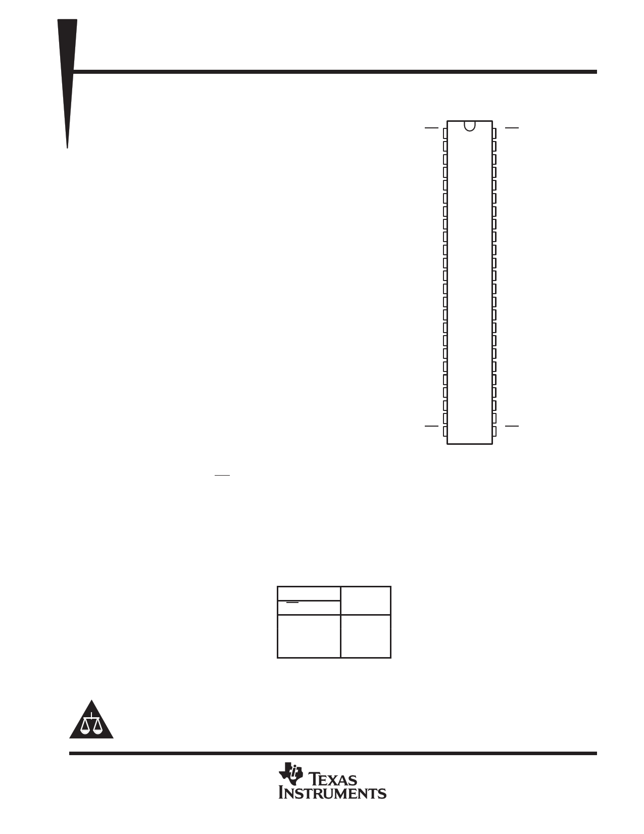
SN54ACT16240 . . . WD PACKAGE
74ACT16240 . . . DL PACKAGE
(TOP VIEW)
1OE
1Y1
1Y2
GND
1Y3
1Y4
VCC
2Y1
2Y2
GND
2Y3
2Y4
3Y1
3Y2
GND
3Y3
3Y4
VCC
4Y1
4Y2
GND
4Y3
4Y4
4OE
1
2
3
4
5
6
7
8
9
10
11
12
13
14
15
16
17
18
19
20
21
22
23
24
48 2OE
47 1A1
46 1A2
45 GND
44 1A3
43 1A4
42 VCC
41 2A1
40 2A2
39 GND
38 2A3
37 2A4
36 3A1
35 3A2
34 GND
33 3A3
32 3A4
31 VCC
30 4A1
29 4A2
28 GND
27 4A3
26 4A4
25 3OE
The 74ACT16240 is packaged in TI’s shrink small-outline package, which provides twice the I/O pin count and
functionality of standard small-outline packages in the same printed-circuit-board area.
The SN54ACT16240 is characterized for operation over the full military temperature range of –55°C to 125°C.
The 74ACT16240 is characterized for operation from –40°C to 85°C.
FUNCTION TABLE
(each section)
INPUTS
OE A
OUTPUT
Y
LH
L
LL
H
HX
Z
Please be aware that an important notice concerning availability, standard warranty, and use in critical applications of
Texas Instruments semiconductor products and disclaimers thereto appears at the end of this data sheet.
EPIC and Widebus are trademarks of Texas Instruments Incorporated.
UNLESS OTHERWISE NOTED this document contains PRODUCTION
DATA information current as of publication date. Products conform to
specifications per the terms of Texas Instruments standard warranty.
Production processing does not necessarily include testing of all
parameters.
•POST OFFICE BOX 655303 DALLAS, TEXAS 75265
Copyright © 1996, Texas Instruments Incorporated
1
1 page 
SN54ACT16240, 74ACT16240
16-BIT BUFFERS/DRIVERS
WITH 3-STATE OUTPUTS
SCAS137C – JULY 1989 – REVISED NOVEMBER 1996
switching characteristics over recommended operating free-air temperature range,
VCC = 5 V ± 0.5 V (unless otherwise noted) (see Figure 1)
PARAMETER
FROM
(INPUT)
TO
(OUTPUT)
TA = 25°C
SN54ACT16240 74ACT16240
MIN TYP MAX MIN MAX MIN MAX
tPLH
tPHL
tPZH
tPZL
tPHZ
tPLZ
A
OE
OE
2.3 5 7.7
2 9.5 2.3 8.5
Y
4.1 6.7 9.2
3 11.5 4.1 10.2
2.6 5.6 8.5
2 10.1 2.6 9.4
Y
3.3 6.7 10.2
2.5 12.2 3.3 11.4
5.9 8.3 11 4.5 12.7 5.9 12
Y
5.1 7.4 9.9
4 12 5.1 10.7
UNIT
ns
ns
ns
operating characteristics, VCC = 5 V, TA = 25°C
PARAMETER
Cpd Power dissipation capacitance per driver
Outputs enabled
Outputs disabled
TEST CONDITIONS
CL = 50 pF, f = 1 MHz
TYP UNIT
38
pF
9
From Output
Under Test
CL = 50 pF
(see Note A)
PARAMETER MEASUREMENT INFORMATION
500 Ω
500 Ω
2 × VCC
S1 Open
GND
TEST
tPLH/tPHL
tPLZ/tPZL
tPHZ/tPZH
S1
Open
2 × VCC
GND
Input
tPHL
Output
1.5 V
LOAD CIRCUIT
1.5 V
50% VCC
3V
0V
tPLH
VOH
50% VCC
VOL
Output
Control
(low-level
enabling) tPZL
Output
Waveform 1
S1 at 2 × VCC
(see Note B)
Output
Waveform 2
S1 at GND
(see Note B)
tPZH
VOLTAGE WAVEFORMS
1.5 V
1.5 V
tPLZ
50% VCC
tPHZ
20% VCC
50% VCC
80% VCC
VOLTAGE WAVEFORMS
3V
0V
[ VCC
VOL
VOH
[0V
NOTES: A. CL includes probe and jig capacitance.
B. Waveform 1 is for an output with internal conditions such that the output is low except when disabled by the output control.
Waveform 2 is for an output with internal conditions such that the output is high except when disabled by the output control.
C. All input pulses are supplied by generators having the following characteristics: PRR ≤ 1 MHz, ZO = 50 Ω, tr = 3 ns, tf = 3 ns.
D. The outputs are measured one at a time with one input transition per measurement.
Figure 1. Load Circuit and Voltage Waveforms
PRODUCT PREVIEW information concerns products in the formative or
design phase of development. Characteristic data and other
specifications are design goals. Texas Instruments reserves the right to
change or discontinue these products without notice.
•POST OFFICE BOX 655303 DALLAS, TEXAS 75265
5
5 Page | ||
| Páginas | Total 6 Páginas | |
| PDF Descargar | [ Datasheet 74ACT16240MTD.PDF ] | |
Hoja de datos destacado
| Número de pieza | Descripción | Fabricantes |
| 74ACT16240MTD | 16-Bit Inverting Buffer/Line Driver with 3-STATE Outputs | Fairchild Semiconductor |
| Número de pieza | Descripción | Fabricantes |
| SLA6805M | High Voltage 3 phase Motor Driver IC. |
Sanken |
| SDC1742 | 12- and 14-Bit Hybrid Synchro / Resolver-to-Digital Converters. |
Analog Devices |
|
DataSheet.es es una pagina web que funciona como un repositorio de manuales o hoja de datos de muchos de los productos más populares, |
| DataSheet.es | 2020 | Privacy Policy | Contacto | Buscar |