|
|
|
PDF 6811 Data sheet ( Hoja de datos )
| Número de pieza | 6811 | |
| Descripción | DABiC-IV/ 12-BIT SERIAL-INPUT/ LATCHED SOURCE DRIVER | |
| Fabricantes | Allegro MicroSystems | |
| Logotipo | ||
Hay una vista previa y un enlace de descarga de 6811 (archivo pdf) en la parte inferior de esta página. Total 8 Páginas | ||
|
No Preview Available !
6811
PRELIMINARY INFORMATION
(subject to change without notice)
May 15, 2000
A6811xA
OUT11 1
OUT 12 2
BLANKING 3 BLNK
SERIAL
DATA OUT
SERIAL
DATA IN
LOGIC
SUPPLY
4
5
6 VDD
CLOCK 7 CLK
STROBE 8 ST
OUT1 9
OUT2 10
20 OUT 10
19 OUT 9
18 OUT 8
17 OUT7
VBB 16
LOAD
SUPPLY
15 GROUND
14 OUT 6
13 OUT 5
12 OUT 4
11 OUT 3
Dwg. PP-029-5
ABSOLUTE MAXIMUM RATINGS
at TA = 25°C
Logic Supply Voltage, VDD ................... 7.0 V
Driver Supply Voltage, VBB ................... 60 V
Continuous Output Current Range,
IOUT ......................... -40 mA to +15 mA
Input Voltage Range,
VIN ....................... -0.3 V to VDD + 0.3 V
Package Power Dissipation,
PD ........................................ See Graph
Operating Temperature Range, TA
(Suffix ‘E–’) .................. -40°C to +85°C
(Suffix ‘S–’) .................. -20°C to +85°C
Storage Temperature Range,
TS ............................... -55°C to +125°C
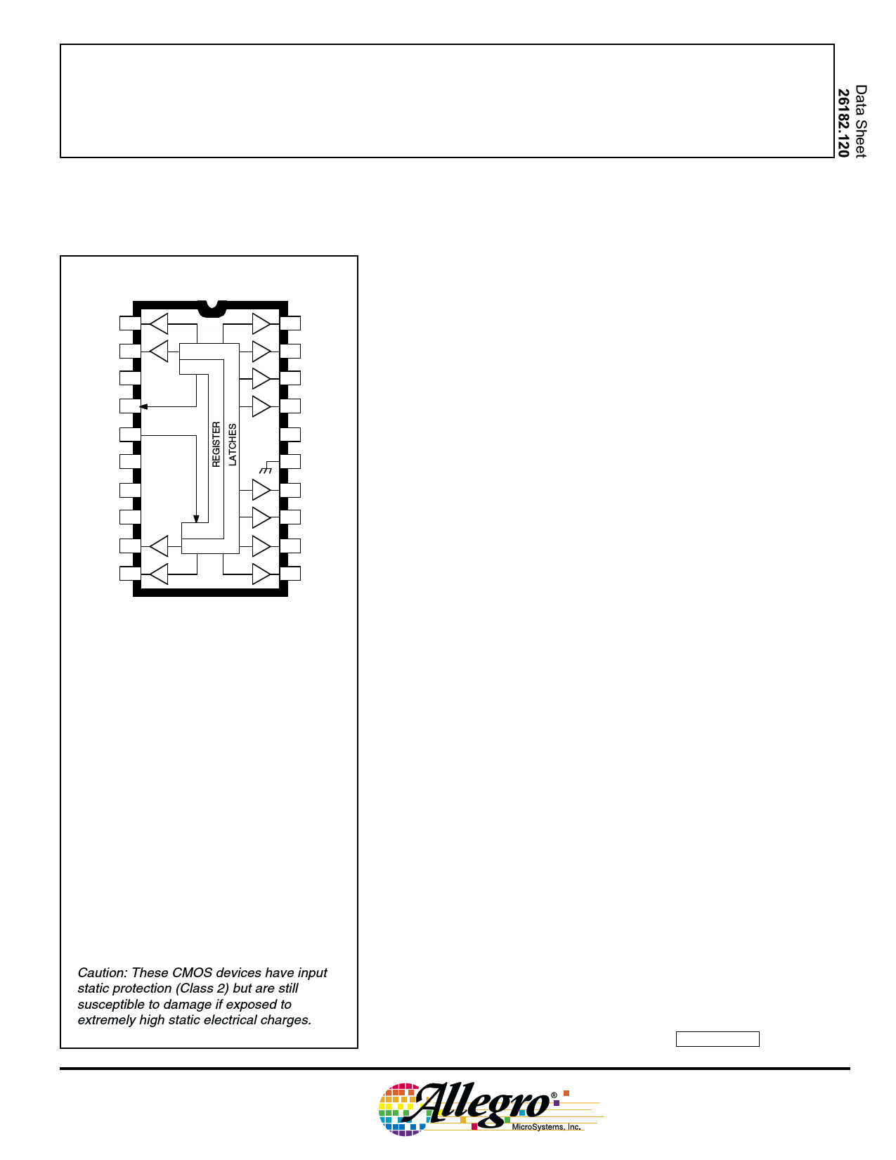
Caution: These CMOS devices have input
static protection (Class 2) but are still
susceptible to damage if exposed to
extremely high static electrical charges.
DABiC-IV, 12-BIT SERIAL-INPUT,
LATCHED SOURCE DRIVER
The A6811– devices combine a 12-bit CMOS shift register,
accompanying data latches and control circuitry with bipolar sourcing
outputs and pnp active pull downs. Designed primarily to drive
vacuum-fluorescent displays, the 60 V and -40 mA output ratings also
allow these devices to be used in many other peripheral power driver
applications. The A6811– features an increased data input rate (com-
pared with the older UCN/UCQ5811A) and a controlled output slew
rate.
The CMOS shift register and latches allow direct interfacing with
microprocessor-based systems. With a 3.3 V or 5 V logic supply,
typical serial-data input rates are up to 33 MHz.
A CMOS serial data output permits cascade connections in applica-
tions requiring additional drive lines. Similar devices are available as
the A6809– and A6810– (10 bits), A6812– (20 bits), and A6818– (32
bits).
The A6811– output source drivers are npn Darlingtons, capable of
sourcing up to 40 mA. The controlled output slew rate reduces electro-
magnetic noise, which is an important consideration in systems that
include telecommunications and/or microprocessors and to meet
government emissions regulations. For inter-digit blanking, all output
drivers can be disabled and all sink drivers turned on with a BLANK-
ING input high. The pnp active pull-downs will sink at least 2.5 mA.
Two temperature ranges are available for optimum performance in
commercial (suffix S-) or industrial (suffix E-) applications. Package
styles are provided for through-hole DIP (suffix -A) and surface-mount
SOIC or PLCC (suffix -LW or -EP). Copper lead frames, low logic-
power dissipation, and low output-saturation voltages allow all devices
to source 25 mA from all outputs continuously at up to 83°C.
FEATURES
I Controlled Output Slew Rate
I High-Speed Data Storage I Low-Power CMOS Logic
I 60 V Minimum
and Latches
Output Breakdown
I Improved Replacements
I High Data Input Rate
for SN75512B, UCN5811–,
I PNP Active Pull-Downs
and UCQ5811–
I Low Output-Saturation Voltages
Complete part number includes a suffix to identify operating
temperature range (E- or S-) and package type (-A, -EP, or -LW).
Always order by complete part number, e.g., A6811SLW .
1 page 
6811
12-BIT SERIAL-INPUT,
LATCHED SOURCE DRIVER
TIMING REQUIREMENTS and SPECIFICATIONS
(Logic Levels are VDD and Ground)
C
CLOCK
50%
SERIAL
DATA IN
SERIAL
DATA OUT
AB
DATA
50%
t p(CH-SQX)
50%
DE
DATA
STROBE
50%
BLANKING
OUT N
LOW = ALL OUTPUTS ENABLED
t p(STH-QH)
t p(STH-QL)
90%
DATA
10%
Dwg. WP-029
BLANKING
OUT N
HIGH = ALL OUTPUTS BLANKED (DISABLED)
50%
t en(BQ)
t dis(BQ)
tr
DATA
10%
tf
90%
A. Data Active Time Before Clock Pulse
(Data Set-Up Time), tsu(D) ......................................... 25 ns
B. Data Active Time After Clock Pulse
(Data Hold Time), th(D) ............................................... 25 ns
C. Clock Pulse Width, tw(CH) ............................................... 50 ns
D. Time Between Clock Activation and Strobe, tsu(C) ....... 100 ns
E. Strobe Pulse Width, tw(STH) ............................................. 50 ns
NOTE – Timing is representative of a 10 MHz clock. Signifi-
cantly higher speeds are attainable.
Serial Data present at the input is transferred to the shift
register on the logic “0” to logic “1” transition of the CLOCK
input pulse. On succeeding CLOCK pulses, the registers shift
data information towards the SERIAL DATA OUTPUT. The
SERIAL DATA must appear at the input prior to the rising edge
of the CLOCK input waveform.
Dwg. WP-030
Information present at any register is transferred to the
respective latch when the STROBE is high (serial-to-parallel
conversion). The latches will continue to accept new data as
long as the STROBE is held high. Applications where the
latches are bypassed (STROBE tied high) will require that the
BLANKING input be high during serial data entry.
When the BLANKING input is high, the output source
drivers are disabled (OFF); the pnp active pull-down sink
drivers are ON. The information stored in the latches is not
affected by the BLANKING input. With the BLANKING input
low, the outputs are controlled by the state of their respective
latches.
www.allegromicro.com
5 Page | ||
| Páginas | Total 8 Páginas | |
| PDF Descargar | [ Datasheet 6811.PDF ] | |
Hoja de datos destacado
| Número de pieza | Descripción | Fabricantes |
| 681 | RECTIFIERS ASSEMBLIES | Microsemi Corporation |
| 681-1 | RECTIFIERS ASSEMBLIES | Microsemi Corporation |
| 681-2 | RECTIFIERS ASSEMBLIES | Microsemi Corporation |
| 681-3 | RECTIFIERS ASSEMBLIES | Microsemi Corporation |
| Número de pieza | Descripción | Fabricantes |
| SLA6805M | High Voltage 3 phase Motor Driver IC. |
Sanken |
| SDC1742 | 12- and 14-Bit Hybrid Synchro / Resolver-to-Digital Converters. |
Analog Devices |
|
DataSheet.es es una pagina web que funciona como un repositorio de manuales o hoja de datos de muchos de los productos más populares, |
| DataSheet.es | 2020 | Privacy Policy | Contacto | Buscar |