|
|
|
PDF WM8214 Data sheet ( Hoja de datos )
| Número de pieza | WM8214 | |
| Descripción | 40MSPS 16 BIT CCD DIGITISER | |
| Fabricantes | Wolfson Microelectronics plc | |
| Logotipo | ||
Hay una vista previa y un enlace de descarga de WM8214 (archivo pdf) en la parte inferior de esta página. Total 30 Páginas | ||
|
No Preview Available !
w
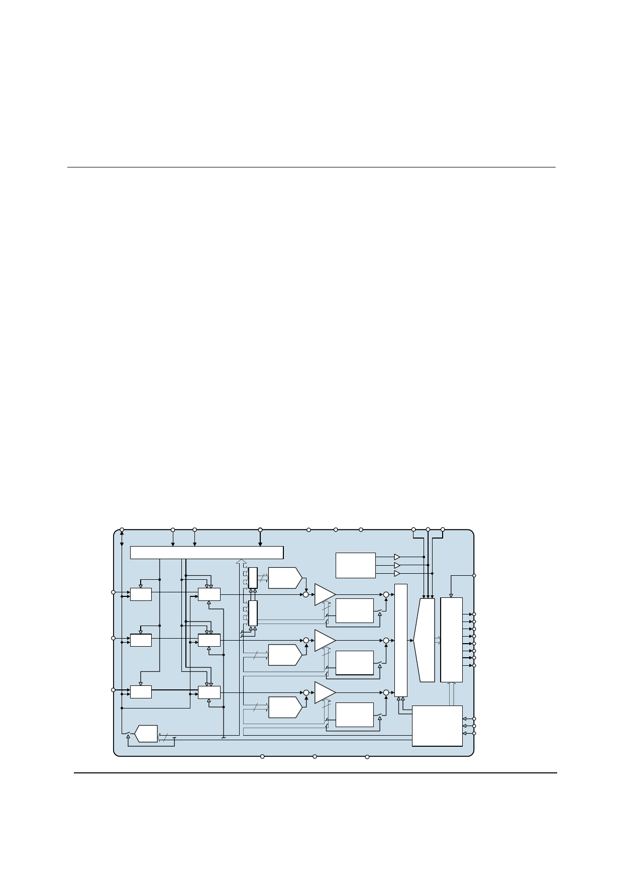
40MSPS 16-bit CCD Digitiser
WM8214
DESCRIPTION
The WM8214 is a 16-bit analogue front end/digitiser IC
which processes and digitises the analogue output signals
from CCD sensors or Contact Image Sensors (CIS) at pixel
sample rates of up to 40MSPS.
The device includes three analogue signal processing
channels each of which contains Reset Level Clamping,
Correlated Double Sampling and Programmable Gain and
Offset adjust functions. Three multiplexers allow single
channel processing. The output from each of these
channels is time multiplexed into a single high-speed 16-bit
Analogue to Digital Converter. The digital output data is
available in 8-bit wide multiplexed format and there is also
an optional single byte output mode, or 4-bit multiplexed
LEGACY mode.
An internal 4-bit DAC is supplied for internal reference level
generation. This may be used during CDS to reference CIS
signals or during Reset Level Clamping to clamp CCD
signals. An external reference level may also be supplied.
ADC references are generated internally, ensuring optimum
performance from the device.
Using an analogue supply voltage of 3.3V and a digital
interface supply of 3.3V, the WM8214 typically only
consumes 390mW.
BLOCK DIAGRAM
FEATURES
• 16-bit ADC
• 40MSPS conversion rate
• Low power – 390mW typical
• 3.3V single supply operation
• Single, 2 or 3 channel operation
• Correlated double sampling
• Programmable gain (9-bit resolution)
• Programmable offset adjust (8-bit resolution)
• Flexible clamp control with programmable clamp voltage
• Flexible timing, can be made compatible with WM819X
and WM815X parts.
• 8-bit wide multiplexed data output format
• 8-bit only output mode
• 4-bit LEGACY multiplexed nibble mode
• Internally generated voltage references
• 28-pin SSOP package, pin compatible with WM8199
• Serial control interface
APPLICATIONS
• High speed USB2.0 compatible scanners
• Multi-function peripherals
• High-performance CCD sensor interface
• Digital Copiers
VRLC/VBIAS
RSMP VSMP
MCLK
AVDD DVDD1 DVDD2
RINP
CLMP RS VS
RLC
TIMING CONTROL
w
WM8214
CDS
RM
GU
X
B
8
OFFSET
DAC
VREF/BIAS
+ PGA
RM
GU
X
B
I/P SIGNAL
9 POLARITY
ADJUST
GINP
RLC
CDS
+ PGA
8 OFFSET
DAC
9 I/P SIGNAL
POLARITY
ADJUST
VRT VRX VRB
+
M
+U
X
16-
BIT
ADC
DATA
O/P
PORT
OEB
OP[0]
OP[1]
OP[2]
OP[3]
OP[4]
OP[5]
OP[6]
OP[7]/SDO
BINP
RLC
RLC 4
DAC
CDS
+ PGA
+
8 OFFSET
DAC
9 I/P SIGNAL
POLARITY
ADJUST
CONFIGURABLE
SERIAL
CONTROL
INTERFACE
SEN
SCK
SDI
WOLFSON MICROELECTRONICS plc
AGND1
AGND2
DGND
Product Preview, March 2004, Rev 1.6
w :: www.wolfsonmicro.com
Copyright 2004 Wolfson Microelectronics plc.
1 page 
Product Preview
WM8214
ABSOLUTE MAXIMUM RATINGS
Absolute Maximum Ratings are stress ratings only. Permanent damage to the device may be caused by continuously operating at
or beyond these limits. Device functional operating limits and guaranteed performance specifications are given under Electrical
Characteristics at the test conditions specified.
ESD Sensitive Device. This device is manufactured on a CMOS process. It is therefore generically susceptible
to damage from excessive static voltages. Proper ESD precautions must be taken during handling and storage
of this device.
Wolfson tests its package types according to IPC/JEDEC J-STD-020B for Moisture Sensitivity to determine acceptable storage
conditions prior to surface mount assembly. These levels are:
MSL1 = unlimited floor life at <30°C / 85% Relative Humidity. Not normally stored in moisture barrier bag.
MSL2 = out of bag storage for 1 year at <30°C / 60% Relative Humidity. Supplied in moisture barrier bag.
MSL3 = out of bag storage for 168 hours at <30°C / 60% Relative Humidity. Supplied in moisture barrier bag.
CONDITION
MIN MAX
Analogue supply voltage: AVDD
GND - 0.3V
GND + 5V
Digital supply voltages: DVDD1 − 2
GND - 0.3V
GND + 5V
Digital ground: DGND
GND - 0.3V
GND + 0.3V
Analogue grounds: AGND1 − 2
GND - 0.3V
GND + 0.3V
Digital inputs, digital outputs and digital I/O pins
GND - 0.3V
DVDD2 + 0.3V
Analogue inputs (RINP, GINP, BINP)
GND - 0.3V
AVDD + 0.3V
Other pins
Operating temperature range: TA
Storage temperature after soldering
GND - 0.3V
0°C
-65°C
AVDD + 0.3V
+70°C
+150°C
Notes:
1. GND denotes the voltage of any ground pin.
2. AGND1, AGND2 and DGND pins are intended to be operated at the same potential. Differential voltages
between these pins will degrade performance.
RECOMMENDED OPERATING CONDITIONS
CONDITION
SYMBOL
MIN
TYP
MAX
UNITS
Operating temperature range
TA 0
70 °C
Analogue supply voltage
AVDD
2.97
3.3
3.63
V
Digital core supply voltage
DVDD1
2.97
3.3
3.63
V
Digital I/O supply voltage
DVDD2
1.8
3.3 3.63
V
Notes:
1. DVDD2 should not be operated at a higher potential than DVDD1.
w
PP Rev 1.6 March 2004
5
5 Page 
Product Preview
WM8214
DEVICE DESCRIPTION
INTRODUCTION
A block diagram of the device showing the signal path is presented on the front page of this
datasheet.
The WM8214 samples up to three inputs (RINP, GINP and BINP) simultaneously. The device then
processes the sampled video signal with respect to the video reset level or an internally/externally
generated reference level using between one and three processing channels.
Each processing channel consists of an Input Sampling block with optional Reset Level Clamping
(RLC) and Correlated Double Sampling (CDS), an 8-bit programmable offset DAC and a 9-bit
Programmable Gain Amplifier (PGA).
The ADC then converts each resulting analogue signal to a 16-bit digital word. The digital output from
the ADC is presented on an 8-bit wide bus.
On-chip control registers determine the configuration of the device, including the offsets and gains
applied to each channel. These registers are programmable via a serial interface.
The WM8214 has been designed to have a high degree of compatibility with previous generations of
Wolfson AFEs. By setting the LEGACY register bit the device adopts the same timing as the
WM819x and WM815x families of AFEs. The control interface is also compatible.
INPUT SAMPLING
The WM8214 can sample and process one to three inputs through one to three processing channels
as follows:
Colour Pixel-by-Pixel: The three inputs (RINP, GINP and BINP) are simultaneously sampled for
each pixel and a separate channel processes each input. The signals are then multiplexed into the
ADC, which converts all three inputs within the pixel period.
Two Channel Pixel-by-pixel: Two input channels (RINP and GINP) are simultaneously sampled for
each pixel and a separate channel processes each input. The signals are then multiplexed into the
ADC, which converts both inputs within the pixel period. The unused Blue channel is powered down
when this mode is selected.
Monochrome: A single chosen input (RINP, GINP, or BINP) is sampled, processed by the
corresponding channel, and converted by the ADC. The choice of input and channel can be changed
via the control interface, e.g. on a line-by-line basis if required. The unused channels are powered
down when this mode is selected.
Colour Line-by-Line: A single input (RINP) is sampled and multiplexed into the red channel for
processing before being converted by the ADC. The registers which are applied to the PGA and
Offset DAC can be switched in turn (RINP → GINP → BINP → RINP…) by applying pulses to the
RSMP pin. This is known as auto-cycling. Alternatively, other sequences can be generated via the
control registers. This mode causes the unused blue and green channels to be powered down. Refer
to the Line-by-Line Operation section for more details.
w
PP Rev 1.6 March 2004
11
11 Page | ||
| Páginas | Total 30 Páginas | |
| PDF Descargar | [ Datasheet WM8214.PDF ] | |
Hoja de datos destacado
| Número de pieza | Descripción | Fabricantes |
| WM8213 | 24MSPS 16-bit CCD Digitiser | Wolfson Microelectronics |
| WM8214 | 40MSPS 16 BIT CCD DIGITISER | Wolfson Microelectronics plc |
| WM8216 | 60MSPS 10-bit 2-channel CCD Digitiser | Wolfson Microelectronics |
| Número de pieza | Descripción | Fabricantes |
| SLA6805M | High Voltage 3 phase Motor Driver IC. |
Sanken |
| SDC1742 | 12- and 14-Bit Hybrid Synchro / Resolver-to-Digital Converters. |
Analog Devices |
|
DataSheet.es es una pagina web que funciona como un repositorio de manuales o hoja de datos de muchos de los productos más populares, |
| DataSheet.es | 2020 | Privacy Policy | Contacto | Buscar |