|
|
|
PDF SDA5648X Data sheet ( Hoja de datos )
| Número de pieza | SDA5648X | |
| Descripción | Decoder for Program Delivery Control and Video Program System PDC / VPS Decoder | |
| Fabricantes | Siemens | |
| Logotipo | ||
Hay una vista previa y un enlace de descarga de SDA5648X (archivo pdf) en la parte inferior de esta página. Total 23 Páginas | ||
|
No Preview Available !
Decoder for Program Delivery
Control and Video Program System
PDC / VPS Decoder
SDA 5648
SDA 5648X
CMOS IC
Features
q Single-chip receiver for PDC data, broadcast either
– in Broadcast Data Service Packet (BDSP) 8/30/2
according to CCIR teletext system B, or
– in dedicated line no. 16 of the vertical blanking interval
(VPS)
q Reception of Unified Date and Time (UDT) broadcast in
BDSP 8/30/1
q Low external components count
q On-chip data and sync slicer
q I2C-Bus interface for communication with external
microcontroller
q Selection of PDC/VPS operating mode software controlled
by I2C-Bus register
q Pin and software compatible to VPS Decoder SDA 5642
q Supply voltage: 5 V ± 10 %
q Video input signal level: 0.7 Vpp to 1.4 Vpp
q Technology: CMOS
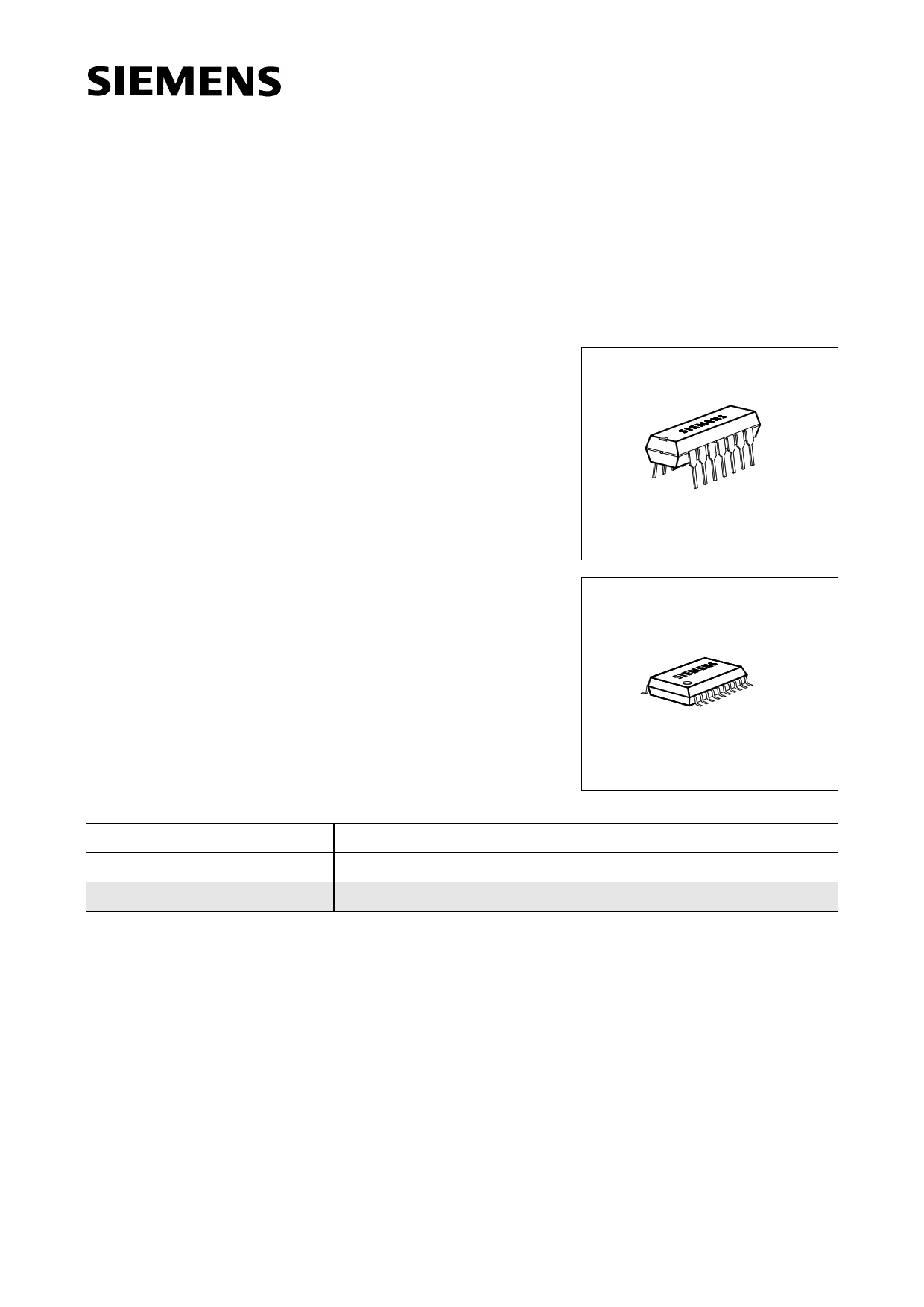
q Package: P-DIP-14-3 and P-DSO-20-1
q Operating temperature range: 0 to 70 °C
P-DIP-14-3
P-DSO-20-1
Type
SDA 5648
SDA 5648X
Ordering Code
Q67000-A5186
Q67006-A5198
Package
P-DIP-14-3
P-DSO-20-1 Tape & Reel
Functional Description
The CMOS circuit SDA 5648 is intended for use in video cassette recorders to retrieve control data
of the PDC system from the data lines broadcast during the vertical blanking interval of a standard
video signal.
The SDA 5648 is devised to handle PDC data transported either in Broadcast Data Service Packet
(BDSP) 8/30 format 2 (bytes no. 13 through 25) of CCIR teletext system B or in the dedicated data
line no. 16 in the case of VPS.
Furthermore it is able to receive the Unified Date and Time (UDT) information transmitted in bytes
no. 15 through 21 of packet 8/30 format 1.
Semiconductor Group
21
12.94
1 page 
SDA 5648
SDA 5648X
Circuit Description
Referring to the functional block diagram of the PDC / VPS decoder, the composite video signal with
negative going sync pulses is coupled to the pin CVBS through a capacitor which is used for
clamping the bottom of the sync pulses to an internally fixed level. The signal is passed on to the
slicer, an analog circuitry separating the sync and the data parts of the CVBS signal, thus yielding
the digital composite sync signal VCS and a digital data signal for further processing by comparing
those signals to internally generated slicing levels.
The output of the sync separator is forwarded, on one hand, to the output pin VCS, and on the other
hand, to the clock generator and the Timing block. The VCS signal represents a key signal that is
used for deriving a system clock signal by means of a PLL.
The data slicer separates the data signal from the CVBS signal by comparing the video voltage to
an internally generated slicing level which is found by averaging the data signal during TV line no.
16 in the VPS mode or by averaging the data signal during the clock run-in period of the teletext
lines during the data entry window (DEW) in PDC mode.
The clock generator delivers the system clock needed for the basic timing as well as for the
regeneration of the data clock. It is based on two phase locked loops (PLL’s) all parts of which are
integrated on chip with the exception of the loop filter components. Each of the PLL’s is composed
of a voltage controlled oscillator (VCO), a phase/frequency detector (PFD), and a charge pump
which converts the digital output signals of the PFD to an analog current. That current is
transformed to a control voltage for the VCO by the off-chip loop filter. The generated VCO fre-
quencies are 10 MHz and 13.875 MHz for VPS mode and PDC mode, respectively.
All signals necessary for the control of sync and data slicing as well as for the data acquisition are
generated by the Timing block.
In PDC mode, only teletext rows 8/30 containing Broadcast Data Service Package (BDSP) infor-
mation are acquired. The relevant bytes of 8/30 format 1 (8/30/1) and 8/30 format 2 (8/30/2) are
extracted. The 8/30/1-bytes are stored in the acquisition register in a transparent way without any
bit manipulation, whereas the Hamming coded bytes of packet 8/30/2 are Hamming-checked and
bytes with one bit error are corrected. The storage of error free or corrected 8/30/2-data bytes in the
transfer register to the I2C-Bus is signalled by the DAVN output going low. The reception and
storage of 8/30/1- data, however, is not indicated by the DAVN output. The presence of 8/30/1 data
can only be checked by polling the data register via the I2C-Bus.
In VPS mode, the extracted data bits of TV line no. 16 are checked for biphase errors. With no
biphase errors encountered, the acquired bytes are stored in the transfer register to the I2C-Bus.
That transfer is signalled by a H/L transition of the DAVN output, as well.
In both operating modes data are updated when a new data line has been received, provided that
the chip is not accessed via the I2C-Bus at the same time.
A micro controller can read the stored bytes via the I2C-Bus interface at any time. However, one
must be aware that the storage of new data from the acquisition interface is inhibited as long as the
PDC decoder is being accessed via the I2C-Bus. At the end of an I2C-Bus reading the transfer
registers are set to FF (hex) until they are updated by the reception of new data packet contained
in the CVBS signal.
Semiconductor Group
25
5 Page 
SDA 5648
SDA 5648X
Description of DAVN and EHB Outputs
DAVN (Data Valid active low)
EHB (First Field active high)
Signal Output
DAVN
H/L-transition
(set low)
L/H-transition
(set high)
always set high
EHB
L/H-transition
H/L-transition
VPS Mode
PDC Mode
8/30/2
8/30/1
in line 16 when
valid VPS data is
received
in the line
carrying
valid
8/30/2 data
in the line
carrying
valid
8/30/1 data
at the start of
line 16
at the beginning of the next field
i.e.,at the start of the next data entry window
on power-up or
during I2C-Bus accesses when the bus master doesn’t
acknowledge in order to generate the stop condition
at the beginning of the first field
at the beginning of the second field
In test mode (i.e. TI = high), both DAVN and EHB are controlled by the CS0 pin and reproduce the
state of the CS0 input.
Semiconductor Group
31
11 Page | ||
| Páginas | Total 23 Páginas | |
| PDF Descargar | [ Datasheet SDA5648X.PDF ] | |
Hoja de datos destacado
| Número de pieza | Descripción | Fabricantes |
| SDA5648 | Decoder for Program Delivery Control and Video Program System PDC / VPS Decoder | Siemens |
| SDA5648X | Decoder for Program Delivery Control and Video Program System PDC / VPS Decoder | Siemens |
| Número de pieza | Descripción | Fabricantes |
| SLA6805M | High Voltage 3 phase Motor Driver IC. |
Sanken |
| SDC1742 | 12- and 14-Bit Hybrid Synchro / Resolver-to-Digital Converters. |
Analog Devices |
|
DataSheet.es es una pagina web que funciona como un repositorio de manuales o hoja de datos de muchos de los productos más populares, |
| DataSheet.es | 2020 | Privacy Policy | Contacto | Buscar |