|
|
|
PDF NE8392C Data sheet ( Hoja de datos )
| Número de pieza | NE8392C | |
| Descripción | Coaxial transceiver interface for Ethernet/Thin Ethernet | |
| Fabricantes | Philipss | |
| Logotipo | ||
Hay una vista previa y un enlace de descarga de NE8392C (archivo pdf) en la parte inferior de esta página. Total 9 Páginas | ||
|
No Preview Available !
Philips Semiconductors
Coaxial transceiver interface for Ethernet/Thin Ethernet
Product specification
NE8392C
DESCRIPTION
The NE8392C Coaxial Transceiver Interface (CTI) is a bipolar
coaxial line driver/receiver for Ethernet (10base5) and Thin Ethernet
(10base2) local area networks. The CTI is connected between the
coaxial cable and the Data Terminal Equipment (DTE) and consists
of a receiver, transmitter, receive-mode collision detector, heartbeat
generator and jabber timer (see Block Diagram). The transmitter
output connects directly to a doubly terminated 50Ω cable, while the
receiver output, collision detector output and transmitter input are
connected to the DTE through isolation transformers. Isolation
between the CTI and the DTE is an IEEE 802.3 requirement that
can be met on signal lines by using a set of pulse transformers
normally available in a standard 16-pin DIP. Power isolation for the
CTI is achieved using DC-to-DC conversion through a power
transformer (see Figure 1, Connection Diagram).
During transmission the jabber timer is initiated to disable the CTI
transmitter in the event of a longer than legal length data packet.
Receive-mode collision detection circuitry monitors the signals on
the coaxial cable to determine the presence of colliding packets and
signals the DTE in the event of a collision. At the end of every
transmission the heartbeat generator creates a pseudo collision for
a short time to ensure that the collision circuitry is functioning
correctly. The heartbeat function can be disabled for repeater
applications.
The CTI is normally part of a three chip set that implements a
complete Ethernet/ Thin Ethernet network interface for a DTE (see
Figure 2, Interface Diagram). The other chips are a Serial Network
Interface (SNI) and a Network Interface Controller (NIC). The SNI
provides Manchester Encoding and Decoding while the NIC handles
the media access protocol and buffer management tasks.
FEATURES
• Compatible with Ethernet II IEEE 802.3 10base5 and 10base2,
and ISO 8802/3 interface specifications
• 100% drop-in compatible with industry standard 8392 sockets
• Integrates all transceiver electronics except signal and power
isolation
• Only one external resistor required for setting coaxial signaling
current
• Jabber timer function integrated on chip
• Heartbeat generator can be externally disabled for operation as
IEEE 802.3 compatible repeaters
ORDERING INFORMATION
DESCRIPTION
16-Pin Plastic Dual In-Line Package (DIP)
28-Pin Plastic Lead Chip Carrier (PLCC)
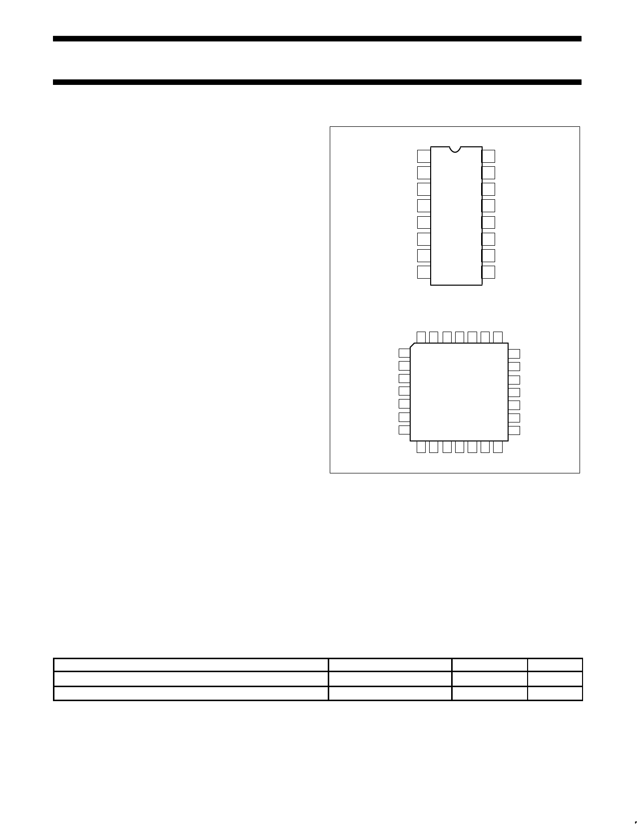
PIN CONFIGURATION
N PACKAGE
CD+ 1
CD– 2
RX+ 3
VEE 4
VEE 5
RX– 6
TX+ 7
TX– 8
16 CDS
15 TXO
14 RXI
13 VEE
12 RR–
11 RR+
10 GND
9 HBE
A PACKAGE
4 3 2 1 28 27 26
VEE 5
V
EE
6
V
EE
7
V
EE
8
VEE 9
VEE 10
V
EE
11
25 V
EE
24 V
EE
23 VEE
22 VEE
21 V
EE
20 V
EE
19 RR–
12 13 14 15 16 17 18
SD00283
• On-chip precision voltage reference for receive mode collision
detection
• Squelch circuitry on all signal inputs rejects noise
• Full ESD protection
• Standard 16-pin DIP and 28-pin PLCC packages
• Power-on reset prevents glitches on coaxial cable during power
up.
• Also available in advanced low-power BiCMOS technology. (See
selection chart and data sheets for the NE83C92, NE83Q92 or
NE83Q93 for appropriate optimal usages)
TEMPERATURE RANGE
0 to +70°C
0 to +70°C
ORDER CODE
NE8392CN
NE8392CA
DWG #
SOT28-4
SOT261-3
1995 May 1
1 853-1693 15180
1 page 
Philips Semiconductors
Coaxial transceiver interface for Ethernet/Thin Ethernet
Product specification
NE8392C
TIMING CHARACTERISTICS
VEE = –9V +5%; TA = 0 to 70°C, unless otherwise specified1. No external isolation diode on TXO.
SYMBOL
tRON
tRD
tRR
tRF
tOS
tRJ
tRHI
tRM
tTST
tTD
tTR
tTF
tTM
tTS
tTON
tTOFF
tCON
tCOFF
tCHI
fCD
tCP
tHON
tHW
tJA
tJR
PARAMETER
Receiver start up delay RXI to RX± (Figure 3)
First received bit on RX±
First validly timed bit on RX±
Receiver prop. delay RXI to RX±
Differential output rise time on RX± and CD±2,3
Differential output fall time on RX± and CD±2,3
Differential output settling time on RX± and CD±
to VOB = 40mV2 (see Figure 4)
Receiver and cable total jitter
Receiver high to idle time
Rise and fall time matching on RX± and CD±
Transmitter start–up delay TX± to TXO
(Figure 5)
First transmitted bit on TXO
First validly timed bit
Transmitter prop delay TX± to TXO
(see Figure 5)
Transmitter rise time 10% to 90% (see Figure 5)
Transmitter fall time 10% to 90% (see Figure 5)
tTF – tTR mismatch
Transmitter added skew4
Transmitter turn on pulse width (see Figure 5)
Transmitter turn off pulse width (see Figure 5)
Collision turn on delay (see Figure 6)
Collision turn off delay (see Figure 6)
Collision high to idle time (see Figure 6)
Collision frequency (see Figure 6)
Collision signal pulse width (see Figure 6)
Heartbeat turn on delay (see Figure 7)
Heartbeat test duration (see Figure 7)
Jabber activation delay measured from TX± to
CD± (see Figure 8)
Jabber reset delay measured from TX± to CD±
(see Figure 8)
TEST CONDITIONS
VRXI = –2V peak
VRXI = –2V peak
Measured to +210mV
tRF – tRR
VTX± = –1V peak
VTX± = 1V peak
VTX± = 1V peak
VTX± = 1V peak
0V to –2V step at RXI
–2V to 0V step at RXI
Measured to +210mV
MIN
150
10
150
150
8.0
35
0.6
0.5
20
250
LIMITS
TYP
35
5
5
1
±3
0.4
MAX
5
tRON +2
50
850
UNIT
bits
ns
ns
ns
µs
ns
ns
ns
1 2 bits
tTST + 2
35 50 ns
25 ns
25 ns
±2 ns
±2 ns
40 ns
250 340 ns
13 bits
16 bits
850 ns
10 12.5 MHz
70 ns
1.6 µs
1.5 µs
60 ms
750 ms
NOTES:
1. All typicals are for VEE = –9V and TA = 27°C.
2. Measured on secondary side of isolation transformer (see Figure 1, Connection Diagram). The transformer has a 1:1 turn ratio with an
inductance between 30 and 100µH at 5MHz.
3. The rise and fall times are measured as the time required for the differential voltage to change from –225mV to +225mV, or +225mV to
–225mV, respectively.
4. Difference in propagation delay between rising and falling edges at TXO.
FUNCTIONAL DESCRIPTION
The NE8392C contains four main functional blocks (see Block
Diagram). These are:
a. The receiver which takes data from the coaxial cable and sends
it to the DTE.
b. The transmitter which receives data from the DTE and sends it
onto the coaxial cable.
c. The collision detection and heartbeat generation circuitry which
indicates to the DTE any collision on the coaxial cable and tests
for collision circuitry functionality at the end of every
transmission.
d. The jabber timer which disables the transmitter in the event of a
longer than legal length data packet.
Receiver Functions
The receiver consists of an input buffer, a cable equalizer, a 4-pole
Bessel low pass filter, a squelch circuit and a differential line driver.
The buffer provides high input resistance and low input capacitance
to minimize loading and reflections on the coaxial cable.
1995 May 1
5
5 Page | ||
| Páginas | Total 9 Páginas | |
| PDF Descargar | [ Datasheet NE8392C.PDF ] | |
Hoja de datos destacado
| Número de pieza | Descripción | Fabricantes |
| NE8392 | Coaxial transceiver interface for Ethernet/Thin Ethernet | Philipss |
| NE8392C | Coaxial transceiver interface for Ethernet/Thin Ethernet | Philipss |
| Número de pieza | Descripción | Fabricantes |
| SLA6805M | High Voltage 3 phase Motor Driver IC. |
Sanken |
| SDC1742 | 12- and 14-Bit Hybrid Synchro / Resolver-to-Digital Converters. |
Analog Devices |
|
DataSheet.es es una pagina web que funciona como un repositorio de manuales o hoja de datos de muchos de los productos más populares, |
| DataSheet.es | 2020 | Privacy Policy | Contacto | Buscar |