|
|
|
PDF NCV8184 Data sheet ( Hoja de datos )
| Número de pieza | NCV8184 | |
| Descripción | Micropower 70 mA Low Dropout Tracking Regulator/Line Driver | |
| Fabricantes | ON | |
| Logotipo | ||
Hay una vista previa y un enlace de descarga de NCV8184 (archivo pdf) en la parte inferior de esta página. Total 20 Páginas | ||
|
No Preview Available !
NCV8184
Micropower 70 mA
Low Dropout Tracking
Regulator/Line Driver
The NCV8184 is a monolithic integrated low dropout tracking
voltage regulator designed to provide an adjustable buffered output
voltage that closely tracks (±3.0 mV) the reference input.
The part can be used in automotive applications with remote
sensors, or any situation where it is necessary to isolate the output of
your regulator.
The NCV8184 also enables the user to bestow a quick upgrade to
their module when added current is needed, and the existing regulator
cannot provide.
The versatility of this part also enables it to be used as a high−side
driver.
Features
• 70 mA Source Capability
• Output Tracks within ±3.0 mV
• Low Input Voltage Tracking Performance
(Works Down to VREF = 2.1 V)
• Low Dropout (0.35 V Typ. @ 50 mA)
• Low Quiescent Current
• Thermal Shutdown
• Wide Operating Range
• Internally Fused Leads in SOIC−8 Package
• NCV Prefix for Automotive and Other Applications Requiring
Unique Site and Control Change Requirements; AEC−Q100
Qualified and PPAP Capable
• These Devices are Pb−Free and are RoHS Compliant
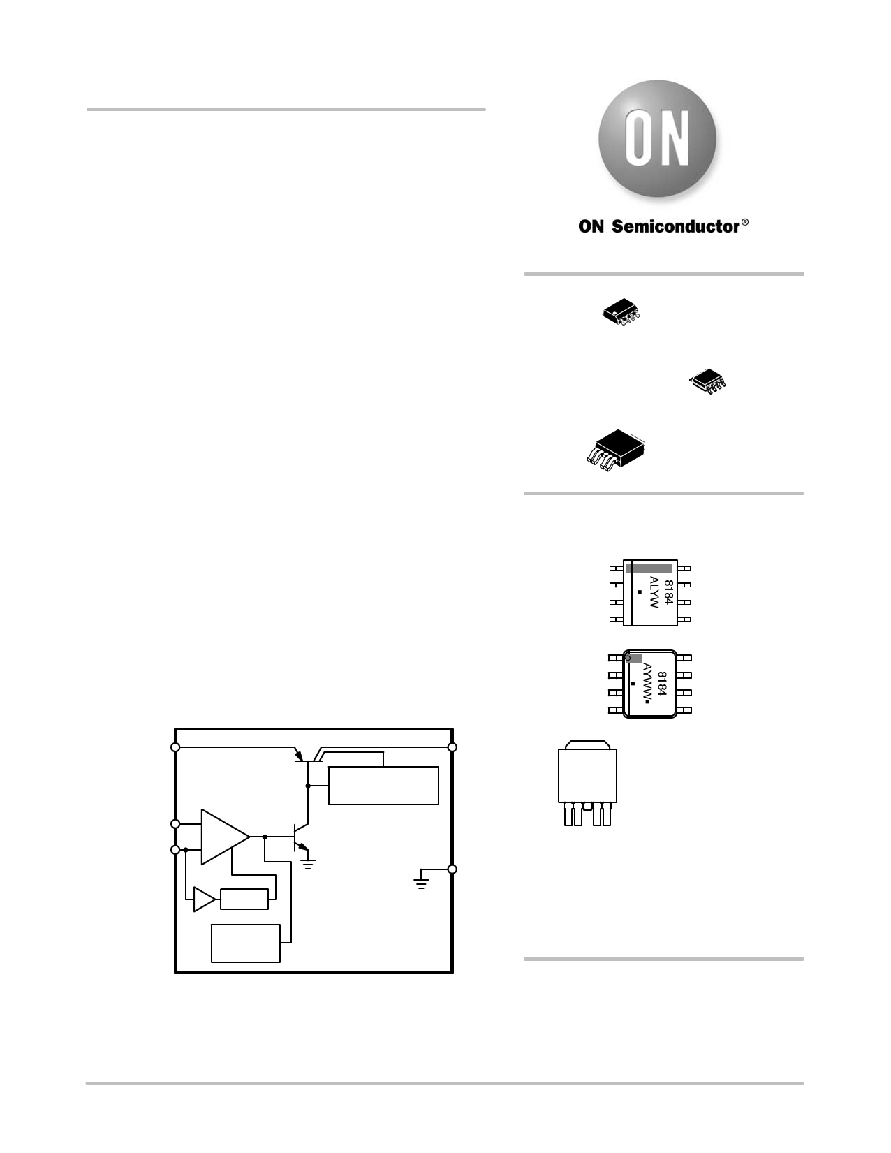
VIN
Adj
VREF/ENABLE
−
+
BIAS
Thermal
Shutdown
Current Limit &
Saturation Sense
VOUT
GND
Figure 1. Block Diagram
http://onsemi.com
SOIC−8
D SUFFIX
1 CASE 751
SOIC−8 EP
PD SUFFIX 8
CASE 751AC
1
DPAK 5−LEAD
DT SUFFIX
1 CASE 175AA
PIN CONNECTIONS AND
MARKING DIAGRAMS
VOUT
GND
GND
Adj
1
VIN
GND
GND
VREF/ENABLE
VOUT
NC
GND
Adj
1
8
VIN
NC
NC
VREF/ENABLE
8184G
ALYWW
Pin 1. VIN
2. VOUT
Tab, 3. GND
4. Adj
5. VREF/ENABLE
1
8184
A
L
Y
W, WW
G or G
= Device Code
= Assembly Location
= Wafer Lot
= Year
= Work Week
= Pb−Free Package
ORDERING INFORMATION
See detailed ordering and shipping information in the package
dimensions section on page 17 of this data sheet.
© Semiconductor Components Industries, LLC, 2012
October, 2012 − Rev. 27
1
Publication Order Number:
NCV8184/D
1 page 
NCV8184
CIRCUIT DESCRIPTION
ENABLE Function
By pulling the VREF/ENABLE lead below 0.8 V, (see
Figure 16 or Figure 17), the IC is disabled and enters a sleep
state where the device draws less than 20 mA from supply.
When the VREF/ENABLE lead is greater than 2.1 V, VOUT
tracks the VREF/ENABLE lead normally.
Output Voltage
The output is capable of supplying 70 mA to the load
while configured as a similar (Figure 13), lower (Figure 15),
or higher (Figure 14) voltage as the reference lead. The Adj
lead acts as the inverting terminal of the op amp and the
VREF lead as the non−inverting.
The device can also be configured as a high−side driver as
displayed in Figure 18.
Loads VOUT, 70 mA
C2**
10 mF
VOUT
GND
GND
VIN
GND
GND
Adj VREF/
ENABLE
VOUT + VREF
B+
C1*
1.0 mF
C3***
10 nF
5.0 V
Figure 13. Tracking Regulator at the Same Voltage
Loads VOUT, 70 mA
C2**
10 mF
RF
VOUT
GND
GND
VIN
GND
GND
B+
C1*
1.0 mF
RA
Adj VREF/
ENABLE
C3***
10 nF
VREF
VOUT + VREF(1 ) RREA)
Figure 14. Tracking Regulator at Higher Voltages
Loads VOUT, 70 mA
C2**
10 mF
VOUT
GND
GND
VIN
GND
GND
Adj VREF/
ENABLE
B+
C1*
1.0 mF
C3***
10 nF
R1
R2
VREF
VOUT, 70 mA
C2**
10 mF
VOUT
GND
GND
VIN
GND
GND
Adj VREF/
ENABLE
from MCU
B+
C1*
1.0 mF
C3***
10 nF
R
VREF
VOUT + VREF(R1R)2R2)
Figure 15. Tracking Regulator at Lower Voltages
Figure 16. Tracking Regulator with ENABLE Circuit
6.0 V−40 V
100 nF
70 mA
To Load 10 mF
(e.g. sensor)
VIN NCV8501 VREF (5.0 V)
VOUT
GND
VIN
GND
GND GND
Adj VREF/
ENABLE
C1*
1.0 mF
I/O
C3***
10 nF
70 mA
mC
VOUT
GND
VIN
GND
GND GND
Adj VREF/
ENABLE
C3***
10 nF
VOUT + B ) * VSAT
B+
MCU
Figure 17. Alternative ENABLE Circuit
Figure 18. High−Side Driver
* C1 is required if the regulator is far from the power source filter. In case of power supply generates voltage ripple (e.g. DC-DC con-
verter) a passive low pass filter with C1 value at least 1 mF is required to suppress the ripple. The filter should be designed according
to particular operating conditions and verified in the application.
** C2 is required for stability.
*** C3 is recommended for EMC susceptibility
http://onsemi.com
5
5 Page 
Parameter
SOIC−8 EP Package
Junction−to−Board (Y−JB, YJB)
Junction−to−Pin 6 (tab) (Y−JL6, YJL6)
Junction−to−Ambient (RqJA, qJA)
Package construction
Without mold compound
NCV8184
PACKAGE THERMAL DATA
Conditions
Typical Value
100 mm2 Spreader Board
645 mm2 Spreader Board
1 oz 2 oz 1 oz 2 oz
26 26 26 25
48 45 37 34
140 123 88 78
Units
°C/W
°C/W
°C/W
Figure 28. PCB Layout and Package Construction for Simulation
http://onsemi.com
11
11 Page | ||
| Páginas | Total 20 Páginas | |
| PDF Descargar | [ Datasheet NCV8184.PDF ] | |
Hoja de datos destacado
| Número de pieza | Descripción | Fabricantes |
| NCV8184 | Micropower 70 mA Low Dropout Tracking Regulator/Line Driver | ON |
| NCV8186 | Fast Transient Response Low Voltage 1A LDO | ON Semiconductor |
| Número de pieza | Descripción | Fabricantes |
| SLA6805M | High Voltage 3 phase Motor Driver IC. |
Sanken |
| SDC1742 | 12- and 14-Bit Hybrid Synchro / Resolver-to-Digital Converters. |
Analog Devices |
|
DataSheet.es es una pagina web que funciona como un repositorio de manuales o hoja de datos de muchos de los productos más populares, |
| DataSheet.es | 2020 | Privacy Policy | Contacto | Buscar |