|
|
|
PDF NDC7001 Data sheet ( Hoja de datos )
| Número de pieza | NDC7001 | |
| Descripción | Dual N & P-Channel Enhancement Mode Field Effect Transistor | |
| Fabricantes | Fairchild | |
| Logotipo | ||
Hay una vista previa y un enlace de descarga de NDC7001 (archivo pdf) en la parte inferior de esta página. Total 13 Páginas | ||
|
No Preview Available !
March 1996
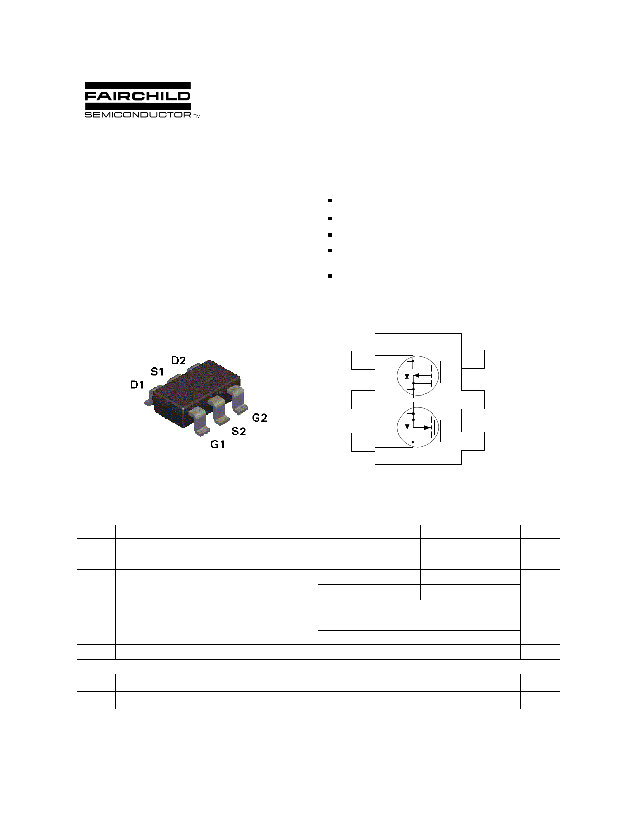
NDC7001C
Dual N & P-Channel Enhancement Mode Field Effect Transistor
General Description
These dual N and P-channel enhancement mode power field
effect transistors are produced using Fairchild's proprietary,
high cell density, DMOS technology. This very high density
process has been designed to minimize on-state resistance,
provide rugged and reliable performance and fast switching.
These devices is particularly suited for low voltage, low
current, switching, and power supply applications.
Features
N-Channel 0.51A, 50V, RDS(ON) = 2Ω @ VGS=10V
P-Channel -0.34A, -50V. RDS(ON)= 5Ω @ VGS=-10V.
High density cell design for low RDS(ON).
Proprietary SuperSOTTM-6 package design using copper
lead frame for superior thermal and electrical capabilities.
High saturation current.
____________________________________________________________________________________________
SuperSOTTM-6
43
52
61
Absolute Maximum Ratings
Symbol Parameter
TA = 25°C unless otherwise noted
VDSS Drain-Source Voltage
VGSS Gate-Source Voltage - Continuous
ID Drain Current - Continuous
- Pulsed
(Note 1a)
PD Maximum Power Dissipation
(Note 1a)
(Note 1b)
(Note 1c)
TJ,TSTG Operating and Storage Temperature Range
THERMAL CHARACTERISTICS
RθJA
RθJC
Thermal Resistance, Junction-to-Ambient
Thermal Resistance, Junction-to-Case
(Note 1a)
(Note 1)
N-Channel
50
20
0.51
1.5
0.96
0.9
0.7
-55 to 150
130
60
P-Channel
-50
-20
-0.34
-1
Units
V
V
A
W
°C
°C/W
°C/W
© 1997 Fairchild Semiconductor Corporation
NDC7001C.SAM
1 page 
Typical Electrical Characteristics: N-Channel (continued)
1.16
1.12
I D = 250µA
1.08
1.04
1
0.96
0.92
0.88
-50 -25 0 25 50 75 100 125 150
TJ , JUNCTION TEMPERATURE (°C)
Figure 7. N-Channel Breakdown Voltage Variation
with Temperature.
1.5
1 VGS = 0V
0.5
TJ = 125°C
0.1
25°C
0.01
-55°C
0.001
0.2
0.4 0.6 0.8
1
V SD , BODY DIODE FORWARD VOLTAGE (V)
1.2
Figure 8. N-Channel Body Diode Forward Voltage
Variation with Current and Temperature.
100
50
C iss
20
C oss
10
5 C rss
f = 1 MHz
2 V GS = 0V
1
0.1 0.2
0.5 1
2
5 10
VDS , DRAIN TO SOURCE VOLTAGE (V)
20
50
Figure 9. N-Channel Capacitance Characteristics.
10
V = 25V
DS
8 ID = 0.51A
6
4
2
0
0 0.2 0.4 0.6 0.8 1 1.2
Q g , GATE CHARGE (nC)
Figure 10. N-Channel Gate Charge Characteristics.
0.7
VDS = 10V
0.6
0.5
TJ = -55°C
25°C
0.4
125°C
0.3
0.2
0.1
0
0 0.3 0.6 0.9 1.2 1.5
VGS , GATE TO SOURCE VOLTAGE (V)
Figure 11. N-Channel Transconductance Variation
with Drain Current and Temperature.
NDC7001C.SAM
5 Page 
SuperSOTTM-6 Tape and Reel Data and Package Dimensions, continued
SSOT-6 Embossed Carrier Tape
Configuration: Figure 3.0
T
P0
D0
E1
K0
Wc
B0
F
E2
W
Tc
A0 P1 D1
User Direction of Feed
Dimensions are in millimeter
Pkg type
A0
B0
W D0 D1 E1 E2
F
P1 P0
SSOT-6
(8mm)
3.23
+/-0.10
3.18
+/-0.10
8.0
+/-0.3
1.55
+/-0.05
1.125
1.75
+/-0.125 +/-0.10
6.25
min
3.50
+/-0.05
4.0
+/-0.1
4.0
+/-0.1
Notes: A0, B0, and K0 dimensions are determined with respect to the EIA/Jedec RS-481
rotational and lateral movement requirements (see sketches A, B, and C).
20 deg maximum
Typical
component
cavity
B0 center line
20 deg maximum component rotation
Sketch A (Side or Front Sectional View)
Component Rotation
Typical
component
A0 center line
SSOT-6 Reel Configuration: Figure 4.0
Sketch B (Top View)
Component Rotation
K0 T
Wc
1.37
+/-0.10
0.255
+/-0.150
5.2
+/-0.3
Tc
0.06
+/-0.02
0.5mm
maximum
0.5mm
maximum
Sketch C (Top View)
Component lateral movement
W1 Measured at Hub
Dim A
Max
Dim A
max
Dim N
See detail AA
7" Diameter Option
B Min
Dim C
See detail AA
Dim D
W3 min
13" Diameter Option
W2 max Measured at Hub
Tape Size
Reel
Option
8mm
7" Dia
8mm
13" Dia
Dimensions are in inches and millimeters
Dim A Dim B
Dim C
7.00
177.8
13.00
330
0.059
1.5
0.059
1.5
512 +0.020/-0.008
13 +0.5/-0.2
512 +0.020/-0.008
13 +0.5/-0.2
Dim D
0.795
20.2
0.795
20.2
Dim N
2.165
55
4.00
100
Dim W1
0.331 +0.059/-0.000
8.4 +1.5/0
0.331 +0.059/-0.000
8.4 +1.5/0
DETAIL AA
Dim W2
0.567
14.4
0.567
14.4
Dim W3 (LSL-USL)
0.311 – 0.429
7.9 – 10.9
0.311 – 0.429
7.9 – 10.9
July 1999, Rev. C
11 Page | ||
| Páginas | Total 13 Páginas | |
| PDF Descargar | [ Datasheet NDC7001.PDF ] | |
Hoja de datos destacado
| Número de pieza | Descripción | Fabricantes |
| NDC7001 | Dual N & P-Channel Enhancement Mode Field Effect Transistor | Fairchild |
| NDC7001C | Dual N & P-Channel Enhancement Mode Field Effect Transistor | Fairchild |
| NDC7002 | Dual N-Channel Enhancement Mode Field Effect Transistor | Fairchild |
| NDC7002N | Dual N-Channel Enhancement Mode Field Effect Transistor | Fairchild |
| Número de pieza | Descripción | Fabricantes |
| SLA6805M | High Voltage 3 phase Motor Driver IC. |
Sanken |
| SDC1742 | 12- and 14-Bit Hybrid Synchro / Resolver-to-Digital Converters. |
Analog Devices |
|
DataSheet.es es una pagina web que funciona como un repositorio de manuales o hoja de datos de muchos de los productos más populares, |
| DataSheet.es | 2020 | Privacy Policy | Contacto | Buscar |