|
|
|
PDF NTR1P02T1 Data sheet ( Hoja de datos )
| Número de pieza | NTR1P02T1 | |
| Descripción | Power MOSFET ( Transistor ) | |
| Fabricantes | ON Semiconductor | |
| Logotipo | ||
Hay una vista previa y un enlace de descarga de NTR1P02T1 (archivo pdf) en la parte inferior de esta página. Total 6 Páginas | ||
|
No Preview Available !
NTR1P02T1
Power MOSFET
−20 V, −1 A, P−Channel SOT−23 Package
Features
• Ultra Low On−Resistance Provides Higher Efficiency
and Extends Battery Life
RDS(on) = 0.180 W, VGS = −10 V
RDS(on) = 0.280 W, VGS = −4.5 V
• Power Management in Portable and Battery−Powered Products
• Miniature SOT−23 Surface Mount Package Saves Board Space
• Mounting Information for SOT−23 Package Provided
Applications
• DC−DC Converters
• Computers
• Printers
• PCMCIA Cards
• Cellular and Cordless Telephones
MAXIMUM RATINGS (TJ = 25°C unless otherwise noted)
Rating
Symbol Value Unit
Drain−to−Source Voltage
Gate−to−Source Voltage − Continuous
Drain Current
− Continuous @ TA = 25°C
− Pulsed Drain Current (tp ≤ 1 ms)
Total Power Dissipation @ TA = 25°C
Operating and Storage Temperature Range
VDSS
VGS
ID
IDM
PD
TJ, Tstg
−20
±20
−1.0
−2.67
400
− 55 to
150
V
V
A
mW
°C
Thermal Resistance − Junction−to−Ambient
Maximum Lead Temperature for Soldering
Purposes, (1/8″ from case for 10 s)
RqJA
TL
300 °C/W
260 °C
Maximum ratings are those values beyond which device damage can occur.
Maximum ratings applied to the device are individual stress limit values (not
normal operating conditions) and are not valid simultaneously. If these limits are
exceeded, device functional operation is not implied, damage may occur and
reliability may be affected.
http://onsemi.com
V(BR)DSS
−20 V
RDS(on) TYP
148 mW @ −10 V
ID MAX
−1.0 A
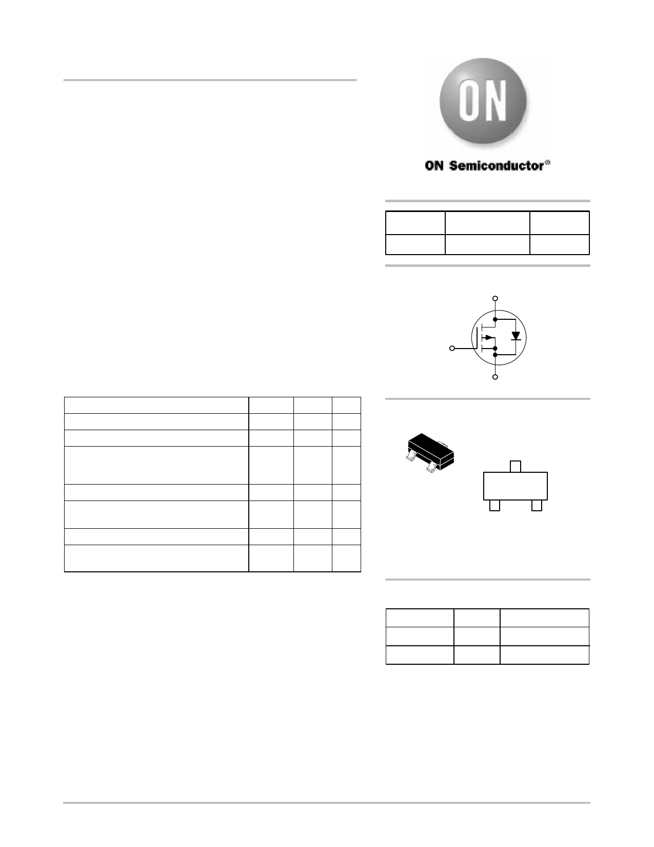
P−Channel
D
G
S
3
1
2
SOT−23
CASE 318
STYLE 21
MARKING DIAGRAM/
PIN ASSIGNMENT
3
Drain
P2W
1
Gate
2
Source
P2 = Specific Device Code
W = Work Week
ORDERING INFORMATION
Device
Package
Shipping†
NTR1P02T1
SOT−23 3000/Tape & Reel
NTR1P02T3
SOT−23 10,000/Tape & Reel
†For information on tape and reel specifications,
including part orientation and tape sizes, please
refer to our Tape and Reel Packaging Specification
Brochure, BRD8011/D.
© Semiconductor Components Industries, LLC, 2004
July, 2004 − Rev. 3
1
Publication Order Number:
NTR1P02T1/D
1 page 
A
L
3
12
BS
VG
C
DH
NTR1P02T1
PACKAGE DIMENSIONS
SOT−23 (TO−236)
CASE 318−09
ISSUE AJ
KJ
NOTES:
1. DIMENSIONING AND TOLERANCING PER ANSI
Y14.5M, 1982.
2. CONTROLLING DIMENSION: INCH.
3. MAXIUMUM LEAD THICKNESS INCLUDES LEAD
FINISH THICKNESS. MINIMUM LEAD
THICKNESS IS THE MINIMUM THICKNESS OF
BASE MATERIAL.
4. 318−01, −02, AND −06 OBSOLETE, NEW
STANDARD 318−09.
INCHES
DIM MIN
MAX
A 0.1102 0.1197
B 0.0472 0.0551
C 0.0385 0.0498
D 0.0140 0.0200
G 0.0670 0.0826
H 0.0040 0.0098
J 0.0034 0.0070
K 0.0180 0.0236
L 0.0350 0.0401
S 0.0830 0.0984
V 0.0177 0.0236
MILLIMETERS
MIN MAX
2.80
3.04
1.20
1.40
0.99
1.26
0.36
0.50
1.70
2.10
0.10
0.25
0.085 0.177
0.45
0.60
0.89
1.02
2.10
2.50
0.45
0.60
STYLE 21:
PIN 1. GATE
2. SOURCE
3. DRAIN
SOLDERING FOOTPRINT*
0.95
0.037
0.95
0.037
0.9
0.035
0.8
0.031
2.0
0.079
ǒ ǓSCALE 10:1
mm
inches
http://onsemi.com
5
5 Page | ||
| Páginas | Total 6 Páginas | |
| PDF Descargar | [ Datasheet NTR1P02T1.PDF ] | |
Hoja de datos destacado
| Número de pieza | Descripción | Fabricantes |
| NTR1P02T1 | Power MOSFET ( Transistor ) | ON Semiconductor |
| NTR1P02T1G | Power MOSFET ( Transistor ) | ON Semiconductor |
| NTR1P02T3 | Power MOSFET ( Transistor ) | ON Semiconductor |
| NTR1P02T3G | Power MOSFET ( Transistor ) | ON Semiconductor |
| Número de pieza | Descripción | Fabricantes |
| SLA6805M | High Voltage 3 phase Motor Driver IC. |
Sanken |
| SDC1742 | 12- and 14-Bit Hybrid Synchro / Resolver-to-Digital Converters. |
Analog Devices |
|
DataSheet.es es una pagina web que funciona como un repositorio de manuales o hoja de datos de muchos de los productos más populares, |
| DataSheet.es | 2020 | Privacy Policy | Contacto | Buscar |