|
|
|
PDF OP27 Data sheet ( Hoja de datos )
| Número de pieza | OP27 | |
| Descripción | Low-Noise / Precision Operational Amplifier | |
| Fabricantes | Analog Devices | |
| Logotipo | ||
1. OP27 Hay una vista previa y un enlace de descarga de OP27 (archivo pdf) en la parte inferior de esta página. Total 21 Páginas | ||
|
No Preview Available !
Data Sheet
Low Noise, Precision
Operational Amplifier
OP27
FEATURES
PIN CONFIGURATIONS
Low noise: 80 nV p-p (0.1 Hz to 10 Hz), 3 nV/√Hz
Low drift: 0.2 µV/°C
High speed: 2.8 V/µs slew rate, 8 MHz gain bandwidth
Low VOS: 10 µV
CMRR: 126 dB at VCM of ±11 V
High open-loop gain: 1.8 million
Available in die form
GENERAL DESCRIPTION
The OP27 precision operational amplifier combines the low
offset and drift of the OP07 with both high speed and low noise.
Offsets down to 25 µV and maximum drift of 0.6 µV/°C make
the OP27 ideal for precision instrumentation applications. Low
noise, en = 3.5 nV/√Hz, at 10 Hz, a low 1/f noise corner
frequency of 2.7 Hz, and high gain (1.8 million), allow accurate
high-gain amplification of low-level signals. A gain bandwidth
product of 8 MHz and a 2.8 V/µs slew rate provide excellent
dynamic accuracy in high speed, data-acquisition systems.
BAL
BAL 1
–IN 2
OP27
V+
OUT
+IN 3
NC
4V– (CASE)
NC = NO CONNECT
Figure 1. 8-Lead TO-99 (J-Suffix)
VOS TRIM 1
–IN 2
+IN 3
V– 4
OP27
8 VOS TRIM
7 V+
6 OUT
5 NC
NC = NO CONNECT
Figure 2. 8-Lead CERDIP – Glass Hermetic Seal (Z-Suffix),
8-Lead PDIP (P-Suffix), and 8-Lead SOIC (S-Suffix)
A low input bias current of ±10 nA is achieved by use of a bias
current cancellation circuit. Over the military temperature
range, this circuit typically holds IB and IOS to ±20 nA and 15 nA,
respectively.
The output stage has good load driving capability. A guaranteed
swing of ±10 V into 600 Ω and low output distortion make the
OP27 an excellent choice for professional audio applications.
(Continued on Page 3)
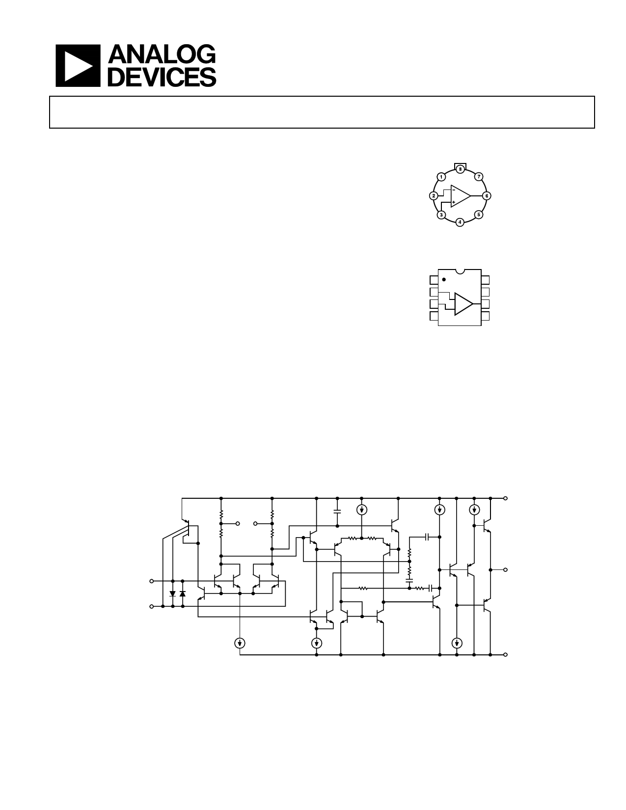
FUNCTIONAL BLOCK DIAGRAM
V+
R3
Q6
R11
18
VOS ADJ.
R4
R21
NONINVERTING
INPUT (+)
INVERTING
INPUT (–)
Q1A Q1B
Q3
1 R1 AND R2 ARE PERMANENTLY
ADJUSTED AT WAFER TEST FOR
MINIMUM OFFSET VOLTAGE
Q2B Q2A
C2
R23 R24
Q22 C1
Q21
Q23 Q24
R9
Q20 Q19
R12
R5 C3 C4
Q11 Q12
Q27
Q28
Q26
Q46
OUTPUT
Q45
V–
Figure 3.
Rev. H
Document Feedback
Information furnished by Analog Devices is believed to be accurate and reliable. However, no
responsibilityisassumedbyAnalogDevices for itsuse,nor foranyinfringementsofpatentsor other
rights of third parties that may result from its use. Specifications subject to change without notice. No
license is granted by implication or otherwise under any patent or patent rights of Analog Devices.
Trademarksandregisteredtrademarksarethepropertyoftheirrespectiveowners.
One Technology Way, P.O. Box 9106, Norwood, MA 02062-9106, U.S.A.
Tel: 781.329.4700 ©1981–2015 Analog Devices, Inc. All rights reserved.
Technical Support
www.analog.com
1 page 
Data Sheet
OP27
VS = ±15 V, −55°C ≤ TA ≤ 125°C, unless otherwise noted.
Table 2.
Parameter
INPUT OFFSET VOLTAGE1
AVERAGE INPUT OFFSET DRIFT
INPUT OFFSET CURRENT
INPUT BIAS CURRENT
INPUT VOLTAGE RANGE
COMMON-MODE REJECTION RATIO
POWER SUPPLY REJECTION RATIO
LARGE SIGNAL VOLTAGE GAIN
OUTPUT VOLTAGE SWING
Symbol
VOS
TCVOS2
TCVOSn3
IOS
IB
IVR
CMRR
PSRR
AVO
VO
Test Conditions
VCM = ±10 V
VS = ±4.5 V to ±18 V
RL ≥ 2 kΩ, VO = ±10 V
RL ≥ 2 kΩ
Min
±10.3
108
600
±11.5
OP27A
Typ
30
Max
60
0.2
15
±20
±11.5
122
2
1200
±13.5
0.6
50
±60
16
Unit
µV
µV/°C
nA
nA
V
dB
µV/V
V/mV
V
1 Input offset voltage measurements are performed by automated test equipment approximately 0.5 seconds after application of power. A/E grades guaranteed fully
warmed up.
2 The TCVOS performance is within the specifications unnulled or when nulled with RP = 8 kΩ to 20 kΩ. TCVOS is 100% tested for A/E grades, sample tested for G grades.
3 Guaranteed by design.
VS = ±15 V, −25°C ≤ TA ≤ 85°C for OP27J and OP27Z and −40°C ≤ TA ≤ 85°C for OP27GS, unless otherwise noted.
Table 3.
Parameter
INPUT ONSET VOLTAGE
AVERAGE INPUT OFFSET DRIFT
INPUT OFFSET CURRENT
INPUT BIAS CURRENT
INPUT VOLTAGE RANGE
COMMON-MODE REJECTION RATIO
POWER SUPPLY REJECTION RATIO
LARGE SIGNAL VOLTAGE GAIN
OUTPUT VOLTAGE SWING
Symbol
VOS
TCVOS1
TCVOSn2
IOS
IB
IVR
CMRR
PSRR
AVO
VO
Test Conditions
VCM = ±10 V
VS = ±4.5 V to ±18 V
RL ≥ 2 kΩ, VO = ±10 V
RL ≥ 2 kΩ
Min
±10.5
110
750
±11.7
OP27E
Typ
20
0.2
0.2
10
±14
±11.8
124
2
1500
±13.6
Max
50
0.6
0.6
50
±60
15
Min
±10.5
96
450
±11.0
OP27G
Typ
55
04
04
20
±25
±11.8
118
2
1000
±13.3
Max
220
1.8
1.8
135
±150
32
Unit
µV
µV/°C
µV/°C
nA
nA
V
dB
µV/V
V/mV
V
1 The TCVOS performance is within the specifications unnulled or when nulled with RP = 8 kΩ to 20 kΩ. TCVOS is 100% tested for A/E grades, sample tested for C/G grades.
2 Guaranteed by design.
Rev. H | Page 5 of 21
5 Page 
Data Sheet
2.5
TA = 25°C
2.0
1.5
1.0
RL = 2kΩ
RL = 1kΩ
0.5
0
0 10 20 30 40 50
TOTAL SUPPLY VOLTAGE (V)
Figure 22. Open-Loop Voltage Gain vs. Supply Voltage
28
TA = 25°C
VS = ±15V
24
20
16
12
8
4
0
1k 10k 100k 1M
FREQUENCY (Hz)
Figure 23. Maximum Output Swing vs. Frequency
10M
18
16
14 POSITIVE
SWING
12
10 NEGATIVE
SWING
8
6
4
2
0
–2
100
1k
LOAD RESISTANCE (Ω)
TA = 25°C
VS = ±15V
10k
Figure 24. Maximum Output Voltage vs. Load Resistance
OP27
100
VS = ±15V
VIN = 100mV
AV = +1
80
60
40
20
0
0
500
1000
1500
2000
2500
CAPACITIVE LOAD (pF)
Figure 25. Small-Signal Overshoot vs. Capacitive Load
50mV
20mV
0V
500ns
AVCL = +1
CL = 15pF
VS = ±15V
TA = 25°C
–50mV
Figure 26. Small-Signal Transient Response
2V
+5V
0V
2µs
AVCL = +1
VS = ±15V
TA = 25°C
–5V
Figure 27. Large Signal Transient Response
Rev. H | Page 11 of 21
11 Page | ||
| Páginas | Total 21 Páginas | |
| PDF Descargar | [ Datasheet OP27.PDF ] | |
Hoja de datos destacado
| Número de pieza | Descripción | Fabricantes |
| OP20 | Micropower Operational Amplifier | PMI |
| OP20 | Micropower Operational Amplifier | Analog |
| OP200 | Dual Low Offset / Low Power Operational Amplifier | Analog Devices |
| OP200 | Infrared Light Emitting Diode | OPTEK Technologies |
| Número de pieza | Descripción | Fabricantes |
| SLA6805M | High Voltage 3 phase Motor Driver IC. |
Sanken |
| SDC1742 | 12- and 14-Bit Hybrid Synchro / Resolver-to-Digital Converters. |
Analog Devices |
|
DataSheet.es es una pagina web que funciona como un repositorio de manuales o hoja de datos de muchos de los productos más populares, |
| DataSheet.es | 2020 | Privacy Policy | Contacto | Buscar |