|
|
|
PDF OP497 Data sheet ( Hoja de datos )
| Número de pieza | OP497 | |
| Descripción | Precision Picoampere Input Current Quad Operational Amplifier | |
| Fabricantes | Analog Devices | |
| Logotipo | ||
Hay una vista previa y un enlace de descarga de OP497 (archivo pdf) en la parte inferior de esta página. Total 12 Páginas | ||
|
No Preview Available !
a
Precision Picoampere Input Current
Quad Operational Amplifier
OP497
FEATURES
Low Offset Voltage: 50 V max
Low Offset Voltage Drift: 0.5 V/؇C max
Very Low Bias Current
25؇C: 100 pA max
–55؇C to +125؇C: 450 pA max
Very High Open-Loop Gain: 2000 V/mV min
Low Supply Current (per Amplifier): 625 A max
Operates from ؎2 V to ؎20 V Supplies
High Common-Mode Rejection: 120 dB min
APPLICATIONS
Strain Gage and Bridge Amplifiers
High Stability Thermocouple Amplifiers
Instrumentation Amplifiers
Photo-Current Monitors
High Gain Linearity Amplifiers
Long-Term Integrators/Filters
Sample-and-Hold Amplifiers
Peak Detectors
Logarithmic Amplifiers
Battery-Powered Systems
GENERAL DESCRIPTION
The OP497 is a quad op amp with precision performance in the
space-saving, industry standard 16-lead SOlC package. Its com-
bination of exceptional precision with low power and extremely
low input bias current makes the quad OP497 useful in a wide
variety of applications.
Precision performance of the OP497 includes very low offset,
under 50 µV, and low drift, below 0.5 µV/°C. Open-loop gain
exceeds 2000 V/mV ensuring high linearity in every application.
Errors due to common-mode signals are eliminated by the OP497’s
common-mode rejection of over 120 dB. The OP497’s power
supply rejection of over 120 dB minimizes offset voltage changes
experienced in battery-powered systems. Supply current of the
OP497 is under 625 µA per amplifier, and it can operate with
supply voltages as low as ± 2 V.
The OP497 utilizes a superbeta input stage with bias current can-
cellation to maintain picoamp bias currents at all temperatures.
This is in contrast to FET input op amps whose bias currents start
in the picoamp range at 25°C, but double for every 10°C rise in
temperature, to reach the nanoamp range above 85°C. Input bias
current of the OP497 is under 100 pA at 25°C and is under 450
pA over the military temperature range.
Combining precision, low power, and low bias current, the
OP497 is ideal for a number of applications, including instru-
mentation amplifiers, log amplifiers, photo-diode preamplifiers,
and long-term integrators. For a single device, see the OP97; for a
dual device, see the OP297.
REV. D
Information furnished by Analog Devices is believed to be accurate and
reliable. However, no responsibility is assumed by Analog Devices for its
use, nor for any infringements of patents or other rights of third parties that
may result from its use. No license is granted by implication or otherwise
under any patent or patent rights of Analog Devices.
PIN CONNECTIONS
16-Lead Wide Body SOIC
(S-Suffix)
OUT A 1
–IN A 2
+IN A 3
V+ 4
+IN B 5
–IN B 6
OUT B 7
NC 8
–+
+–
OP497
–+
16 OUT D
15 –IN D
14 +IN D
13 V–
12 +IN C
11 –IN C
10 OUT C
9 NC
NC = NO CONNECT
14-Lead Plastic Dip
(P-Suffix)
14-Lead Ceramic Dip
(Y-Suffix)
OUT A 1
–IN A 2
+IN A 3
V+ 4
+IN B 5
–IN B 6
OUT B 7
–+ +–
OP497
–+
14 OUT D
13 –IN D
12 +IN D
11 V–
10 +IN C
9 –IN C
8 OUT C
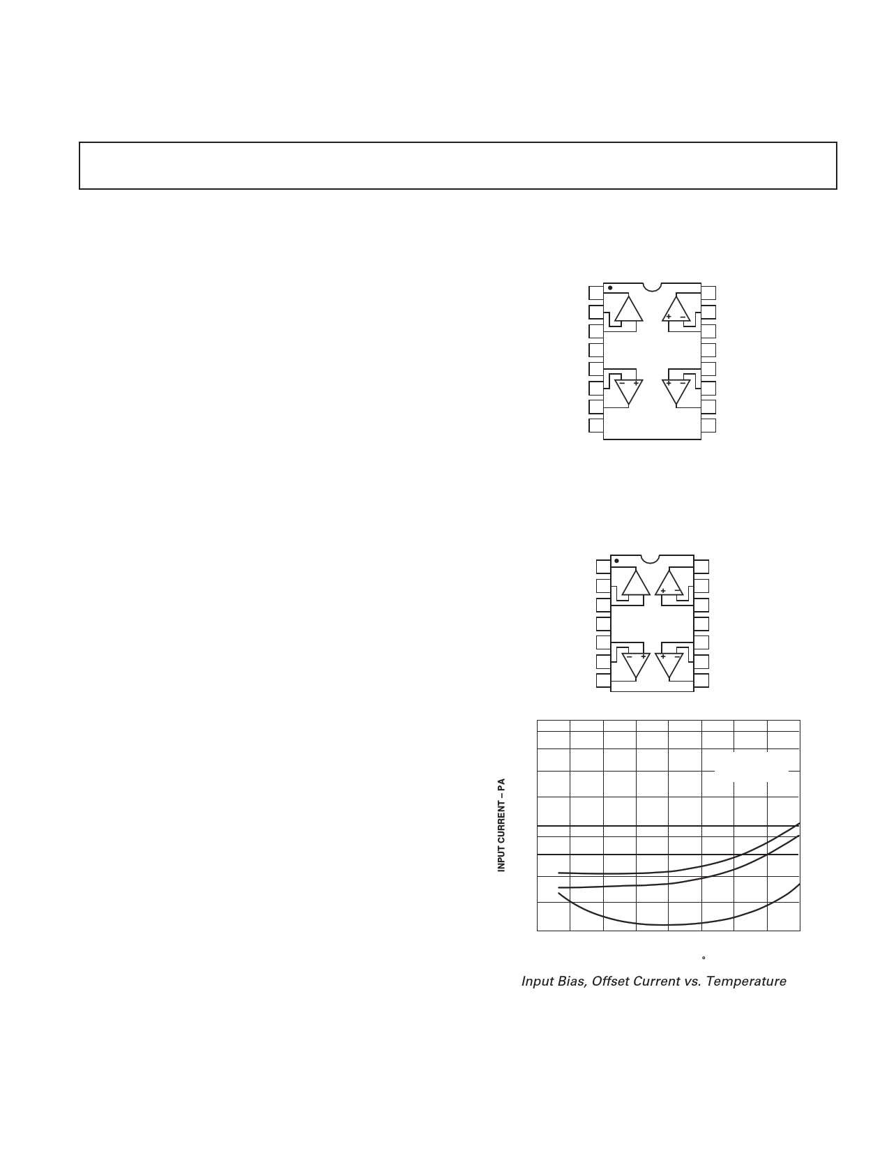
1000
VS = ؎15V
VCM = 0V
100
–IB
+IB
IOS
10
–75 –50 –25 0 25 50 75 100 125
TEMPERATURE – C
Input Bias, Offset Current vs. Temperature
One Technology Way, P.O. Box 9106, Norwood, MA 02062-9106, U.S.A.
Tel: 781/329-4700
www.analog.com
Fax: 781/326-8703
© Analog Devices, Inc., 2002
1 page 
1000
TA = 25؇C
VS = 2V TO 20V
100
CURRENT NOISE
VOLTAGE NOISE
10
1
1 10 100 1000
FREQUENCY – Hz
TPC 10. Voltage Noise Density
vs. Frequency
10
TA = 25؇C
VS = ؎2V TO ؎20V
1
0.1
10Hz
1kHz
0.01
102
103 104 105 106
SOURCE RESISTANCE – ⍀
107
TPC 11. Total Noise Density vs.
Source Resistance
5mV
100
90
OP497
1s
10
0% VS = 15V
TA = 25؇C
02 4
6 8 10
TIME – Secs
TPC 12. 0.1 Hz to 10 Hz Noise Voltage
100
80
GAIN
60
PHASE
40
VS = ؎15V
CL = 30pF
RL = 1M⍀
TA = 25؇C
90
20 135
0 180
–20 225
–40
100
1k 10k 100k 1M
FREQUENCY – Hz
10M
TPC 13. Open-Loop Gain,
Phase vs. Frequency
10000
1000
TA = –55؇C
TA = +25C
TA = +125؇C
100
1
VS = ؎15V
VO = ؎10V
10
LOAD RESISTANCE – k⍀
20
TPC 14. Open-Loop Gain vs.
Load Resistance
RL = 2k⍀
VS = ؎15V
VCN = ؎10V
TA= +125؇C
TA= +25؇C
TA= –55؇C
–15 –10 –5
0
5 10
OUTPUT VOLTAGE – V
15
TPC 15. Open-Loop Gain Linearity
160
VS = ؎15V
140 TA= 25؇C
120
100
80
60
40
20
0
1 10 100 1k 10k 100k 1M
FREQUENCY – Hz
TPC 16. Common-Mode
Rejection vs. Frequency
160
VS = ؎15V
140 TA = 25؇C
120
–PSR
100
+PSR
80
60
40
20
0
1 10 100 1k 10k 100k 1M
FREQUENCY – Hz
TPC 17. Power Supply
Rejection vs. Frequency
35
VS= ؎15V
30 TA= 25؇C
AVCL= +1
1%THD
25 RL = 10k⍀
20
15
10
5
0
100 1k 10k 100k
FREQUENCY – Hz
TPC 18. Maximum Output
Swing vs. Frequency
REV. D
–5–
5 Page 
Table I. OP497 SPICE Net-List
* Node assignments
* noninverting input
* inverting input
* positive supply
* negative supply
* output
*
*SUBCKT OP497 1 2 99 50 27
*
* INPUT STAGE AND POLE AT 6 MHz
*
RIN1 1 7 2500
RIN2 2 8 2500
R1 8 3 6.782E8
R2 7 3 6.782E8
R3 5 99 542.57
R4 6 99 542.57
CIN 7 8 3E-12
C2 5 6 24.445E-12
I1 4 50 0.1E-3
IOS 7 8 15E-12
EOS 9 7 POLY(1) 16 21 40E-6
1
Q1 5 8 10 QX
Q2 6 9 11 QX
R5 10 4 25.374
R6 11 4 25.374
D1 8 9 DX
D2 9 8 DX
*
EREF 98 0 21 0 1
*
*GAIN STAGE AND DOMINANT POLE AT 0.11 Hz
*
R7 1 98 2.1703E9
C3 2 98 666.67E-12
G1 98 12 5
V1 99 13 1.275
V2 11 9 1.275
D3 12 13 DX
D4 14 12 DX
*
*COMMON-MODE GAIN NETWORK WITH ZERO AT 50 MHz
*
RCM1 15 16 1E6
CCM 15 16 3.18E-9
RCM2 16 98 1
ECM 15 98 3 21 177.83E-3
* NEGATIVE ZERO AT 1.8 MHz
*
E1 17 98 12 21 1E6
R8 17 18 1E6
C4 17 18 –88.419E-15
R9 18 98 1
*
* POLE AT 6 MHz
*
G2 98 19 18 21 1E-6
R15 20 98 1E6
C8 20 98 26.526E-15
*
* POLE AT 1.8 MHz
*
G6 98 20 19 21 1E-6
R20 20 98 1E6
C10 20 98 88.419E-15
*
* OUTPUT STAGE
*
R16 99 21 160 k
R17 21 50 160 k
ISY 99 50 331E-6
V3 23 22 1.9
D5 20 23 DX
V4 22 24 1.9
D6 24 20 DX
D7 99 25 DX
G4 25 50 20 22 5E-3
D9 50 25 DY
D8 99 26 DX
G5 26 50 22 20 5E-3
D10 50 26 DY
G6 22 99 99 20 5E-3
R18 99 22 200
G7 50 22 20 50 5E-3
R19 22 50 200
L1 22 27 0.1E-6
*
* MODELS USED
*
.MODEL QX NPN (BF = 1.25E6)
.MODEL DX (IS = 1E-15)
.MODEL DZ D(IS = 1E-15 BV = 50)
.ENDS OP497
OP497
REV. D
–11–
11 Page | ||
| Páginas | Total 12 Páginas | |
| PDF Descargar | [ Datasheet OP497.PDF ] | |
Hoja de datos destacado
| Número de pieza | Descripción | Fabricantes |
| OP490 | Low Voltage Micropower Quad Operational Amplifier | Analog Devices |
| OP491 | Micropower Single-Supply Rail-to-Rail Input/Output Op Amps | Analog Devices |
| OP492 | DUAL/QUAD SINGLE SUPPLY OPERATIONAL AMPLIFIER | Analog Devices |
| OP493 | Precision / Micropower Operational Amplifiers | Analog Devices |
| Número de pieza | Descripción | Fabricantes |
| SLA6805M | High Voltage 3 phase Motor Driver IC. |
Sanken |
| SDC1742 | 12- and 14-Bit Hybrid Synchro / Resolver-to-Digital Converters. |
Analog Devices |
|
DataSheet.es es una pagina web que funciona como un repositorio de manuales o hoja de datos de muchos de los productos más populares, |
| DataSheet.es | 2020 | Privacy Policy | Contacto | Buscar |