|
|
|
PDF OPA2686 Data sheet ( Hoja de datos )
| Número de pieza | OPA2686 | |
| Descripción | Dual / Wideband / Low Noise / Voltage Feedback OPERATIONAL AMPLIFIER | |
| Fabricantes | Burr-Brown | |
| Logotipo | ||
Hay una vista previa y un enlace de descarga de OPA2686 (archivo pdf) en la parte inferior de esta página. Total 18 Páginas | ||
|
No Preview Available !
® OPA2686
OPA2686
TM Dual, Wideband, Low Noise,
Voltage Feedback OPERATIONAL AMPLIFIER
FEATURES
q HIGH GAIN BANDWIDTH: 1.6GHz
q LOW INPUT VOLTAGE NOISE: 1.4nV/√Hz
q VERY LOW DISTORTION: –90dBc (5MHz)
q LOW SUPPLY CURRENT: 12mA/chan.
q HIGH CHANNEL ISOLATION: 70dB
q ±5V OPERATION
q STABLE FOR GAINS ≥ +7
DESCRIPTION
The OPA2686 provides two very low noise, high gain
bandwidth, voltage feedback op amps in a single
package. Operating from a low 12mA/channel quies-
cent current, each channel provides a 1.4nV/√Hz input
voltage noise with a 1.6GHz gain bandwidth product.
Minimum stable gain is specified at +7V/V while
exceptional flatness is guaranteed at a gain of +10.
The combination of low noise, high slew rate
(600V/µs), and broad bandwidth allow exceptional xDSL
differential receivers to be implemented. Additionally,
de-compensated, low-noise voltage-feedback op amps
are ideal for broadband transimpedance requirements.
APPLICATIONS
q LOW NOISE, DIFFERENTIAL AMPLIFIERS
q xDSL RECEIVER AMPLIFIER
q ULTRASOUND HIGH GAIN PREAMP
q DIFFERENTIAL ADC PREAMP
q MATCHED I AND Q CHANNEL AMPLIFIERS
q MATCHED TRANSIMPEDANCE AMPLIFIERS
q PROFESSIONAL AUDIO DUAL
TRANSIMPEDANCE
The dual channel OPA2686 provides matched channels
for high speed differencing transimpedance require-
ments. With over 200MHz bandwidth at a gain of
20dB, excellent gain and phase matching is provided at
IF frequencies for matched I and Q channel amplifiers.
OPA2686 RELATED PRODUCTS
SINGLES
OPA643
OPA686
OPA687
INPUT NOISE
VOLTAGE (nV/√Hz)
2.3
1.3
0.95
GAIN BANDWIDTH
PRODUCT (MHz)
800
1600
3600
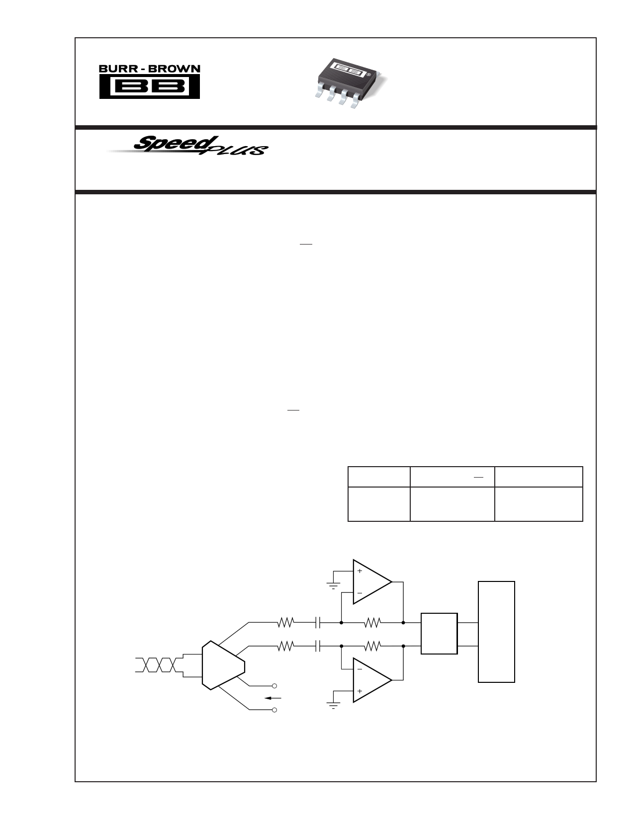
Diplexer
RG
RG
Driver
1/2
OPA2686
RF
RF
1/2
OPA2686
Passive
Filter
Analog
Front
End
Low Noise VDSL Receiver
International Airport Industrial Park • Mailing Address: PO Box 11400, Tucson, AZ 85734 • Street Address: 6730 S. Tucson Blvd., Tucson, AZ 85706 • Tel: (520) 746-1111
Twx: 910-952-1111 • Internet: http://www.burr-brown.com/ • Cable: BBRCORP • Telex: 066-6491 • FAX: (520) 889-1510 • Immediate Product Info: (800) 548-6132
©1998 Burr-Brown Corporation
PDS-11371B
OPPArint2ed6in8U6.S.A. May, 2000
®
1 page 
TYPICAL PERFORMANCE CURVES: VS = ±5V (Cont.)
At TA = +25°C, G = +10, RF = 453Ω, and RL = 100Ω, unless otherwise noted. See Figure 1.
–60
–70
–80
–90
–100
–110
0.1
5MHz 2nd HARMONIC DISTORTION
vs OUTPUT VOLTAGE
RL = 100Ω
RL = 200Ω
RL = 500Ω
1
Output Voltage (Vp-p)
10
–60
–70
–80
–90
–100
–110
0.1
5MHz 3rd HARMONIC DISTORTION
vs OUTPUT VOLTAGE
RL = 200Ω
RL = 100Ω
1
Output Voltage (Vp-p)
RL = 500Ω
10
–55
–60
–65
–70
–75
–80
–85
–90
–95
–100
–105
0.1
10MHz 2nd HARMONIC DISTORTION
vs OUTPUT VOLTAGE
RL = 100Ω
RL = 200Ω
RL = 500Ω
1
Output Voltage (Vp-p)
10
–55
–60
–65
–70
–75
–80
–85
–90
–95
–100
–105
0.1
10MHz 3rd HARMONIC DISTORTION
vs OUTPUT VOLTAGE
RL = 100Ω
RL = 200Ω
RL = 500Ω
1
Output Voltage (Vp-p)
10
–50
–55
–60
–65
–70
–75
–80
–85
–90
–95
0.1
20MHz 2nd HARMONIC DISTORTION
vs OUTPUT VOLTAGE
RL = 100Ω
RL = 200Ω
RL = 500Ω
1
Output Voltage (Vp-p)
10
–50
–55
–60
–65
–70
–75
–80
–85
–90
–95
0.1
20MHz 3rd HARMONIC DISTORTION
vs OUTPUT VOLTAGE
RL = 100Ω
RL = 500Ω
RL = 200Ω
1
Output Voltage (Vp-p)
10
®
5 OPA2686
5 Page 
primary goal, Equation 4 gives a solution for RF in the input
stage that will provide an equal bandwidth in the first and
second stages, giving the maximum overall channel band-
width.
RF
=
2
π
Z 2T
CD GBP
1
/
3
Eq. 4
Where:
ZT = Desired total transimpedance gain
CD = Diode capacitance at reverse bias
GBP = Amplifier Gain Bandwidth Product (MHz)
This equation is used to calculate the required input stage
feedback resistor in Figure 4. The remaining total signal gain
is provided by the second stage; in the example of Figure 4,
setting G = 37.5 gives the same bandwidth (approximately
42MHz) as the bandwidth achieved by the input stage. To
set this first stage bandwidth to its maximally flat values, use
Equation 5 to set the feedback capacitor value:
CF =
π
CD
RF GBP
Eq. 5
( ) ( )f–3dB =
1
2
(GBP)2 / 3
2 π CD 1/ 3 ZT 1/ 3
Eq. 6
The approximate achievable bandwidth in the two stages is
given by Equation 6 which gives approximately 30MHz for
Figure 4.
LOW GAIN COMPENSATION FOR IMPROVED SFDR
Where a low gain is desired, and inverting operation is
acceptable, a new external compensation technique may be
used to retain the full slew rate and noise benefits of the
OPA2686 while giving increased loop gain and the associ-
ated improvement in distortion offered by the decompen-
sated architecture. This technique shapes the loop gain for
good stability while giving an easily controlled second-
order low pass frequency response. Considering only the
noise gain (non-inverting signal gain) for the circuit of
Figure 5, the low frequency noise gain, (NG1) will be set by
+5V
the resistor ratios while the high frequency noise gain (NG2)
will be set by the capacitor ratios. The capacitor values set
both the transition frequencies and the high frequency noise
gain. If this noise gain, determined by NG2 = 1+CS/CF, is set
to a value greater than the recommended minimum stable
gain for the op amp and the noise gain pole, set by 1/RFCF,
is placed correctly, a very well controlled 2nd-order low
pass frequency response will result.
To choose the values for both CS and CF, two parameters and
only three equations need to be solved. The first parameter
is the target high frequency noise gain NG2, which should be
greater than the minimum stable gain for the OPA2686.
Here, a target NG2 of 10.5 will be used. The second param-
eter is the desired low frequency signal gain, which also sets
the low frequency noise gain NG1. To simplify this discus-
sion, we will target a maximally flat second-order low pass
Butterworth frequency response (Q = 0.707). The signal
gain of –2 shown in Figure 5 will set the low frequency noise
gain to NG1 = 1 + RF/RG (NG1= 3 in this example). Then,
using only these two gains and the GBP for the OPA2686
(1600MHz), the key frequency in the compensation can be
determined as:
ZO
=
GBP
NG12
1 –
NG1
NG2
–
1–
2
NG1
NG 2
Eq. 7
Physically, this Z0 (10.6MHz for the values shown above) is
set by 1/(2π • RF(CF + CS)) and is the frequency at which the
rising portion of the noise gain would intersect unity gain if
projected back to 0dB gain. The actual zero in the noise gain
occurs at NG1 • Z0 and the pole in the noise gain occurs at
NG2 • Z0. Since GBP is expressed in Hz, multiply Z0 by 2π
and use this to get CF by solving:
CF
=
2π
•
1
R F Z O NG 2
(= 2.86pF)
Eq. 8
Finally, since CS and CF set the high frequency noise gain,
determine CS by:
CS = (NG2 – 1) CF (= 27.2pF)
Eq. 9
The resulting closed-loop bandwidth will be approximately
equal to:
f –3dB ≅ ZO GBP
(= 130MHz) Eq. 10
RG
250Ω
VI
1/2
OPA2686
RF
500Ω
CS
27pF
–5V
CF
2.9pF
VO
For the values shown in Figure 5, the f–3dB will be approxi-
mately 130MHz. This is less than that predicted by simply
dividing the GBP product by NG1. The compensation
network controls the bandwidth to a lower value while
providing the full slew rate at the output and an excep-
tional distortion performance due to increased loop gain at
frequencies below NG1 • Z0. The capacitor values shown
in Figure 5 are calculated for NG1 = 3 and NG2 = 10.5 with
no adjustment for parasitics.
FIGURE 5. Broadband Low Gain Inverting External
Compensation.
11
OPA2686
®
11 Page | ||
| Páginas | Total 18 Páginas | |
| PDF Descargar | [ Datasheet OPA2686.PDF ] | |
Hoja de datos destacado
| Número de pieza | Descripción | Fabricantes |
| OPA2680 | SpeedPlus Dual Wideband Voltage Feedback Operational Amplifier with Disable | Texas Instruments |
| OPA2680 | Dual Wideband / Voltage Feedback OPERATIONAL AMPLIFIER With Disable | Burr-Brown |
| OPA2681 | OPA2681: SpeedPlus Dual Wideband Current Feedback Op Amp with Disable (Rev. A) | Texas Instruments |
| OPA2681 | Dual Wideband / Current Feedback OPERATIONAL AMPLIFIER With Disable | Burr-Brown |
| Número de pieza | Descripción | Fabricantes |
| SLA6805M | High Voltage 3 phase Motor Driver IC. |
Sanken |
| SDC1742 | 12- and 14-Bit Hybrid Synchro / Resolver-to-Digital Converters. |
Analog Devices |
|
DataSheet.es es una pagina web que funciona como un repositorio de manuales o hoja de datos de muchos de los productos más populares, |
| DataSheet.es | 2020 | Privacy Policy | Contacto | Buscar |