|
|
PDF SA900 Data sheet ( Hoja de datos )
| Número de pieza | SA900 | |
| Descripción | I/Q transmit modulator | |
| Fabricantes | Philips | |
| Logotipo |  |
|
Hay una vista previa y un enlace de descarga de SA900 (archivo pdf) en la parte inferior de esta página. Total 20 Páginas | ||
|
No Preview Available !
INTEGRATED CIRCUITS
SA900
I/Q transmit modulator
Preliminary specification
IC17 Data Handbook
Philips
Semiconductors
1997 Sept 16
1 page 
Philips Semiconductors
I/Q transmit modulator
Preliminary specification
SA900
GND_LO
1
GND GND GND GND GND_CTRL
4 11 16 18
25
GND GND GND GND GND GND GND
28 30 33 35 37 39 45
VCC_LO
48
GND
VCC
5
VCC
8
VCC
14
VCC
27
VCC
29
VCC
32
VCC
36
VCC
38
VCC
44
VCC_CTRL
26
VCC
2
VCC
3
50Ω
50Ω
VCC
6
VCC
7
VCC
9
1997 Sept 16
0.1/6.4 mA
0.1/6.4 mA
VCC
12
VCC
13
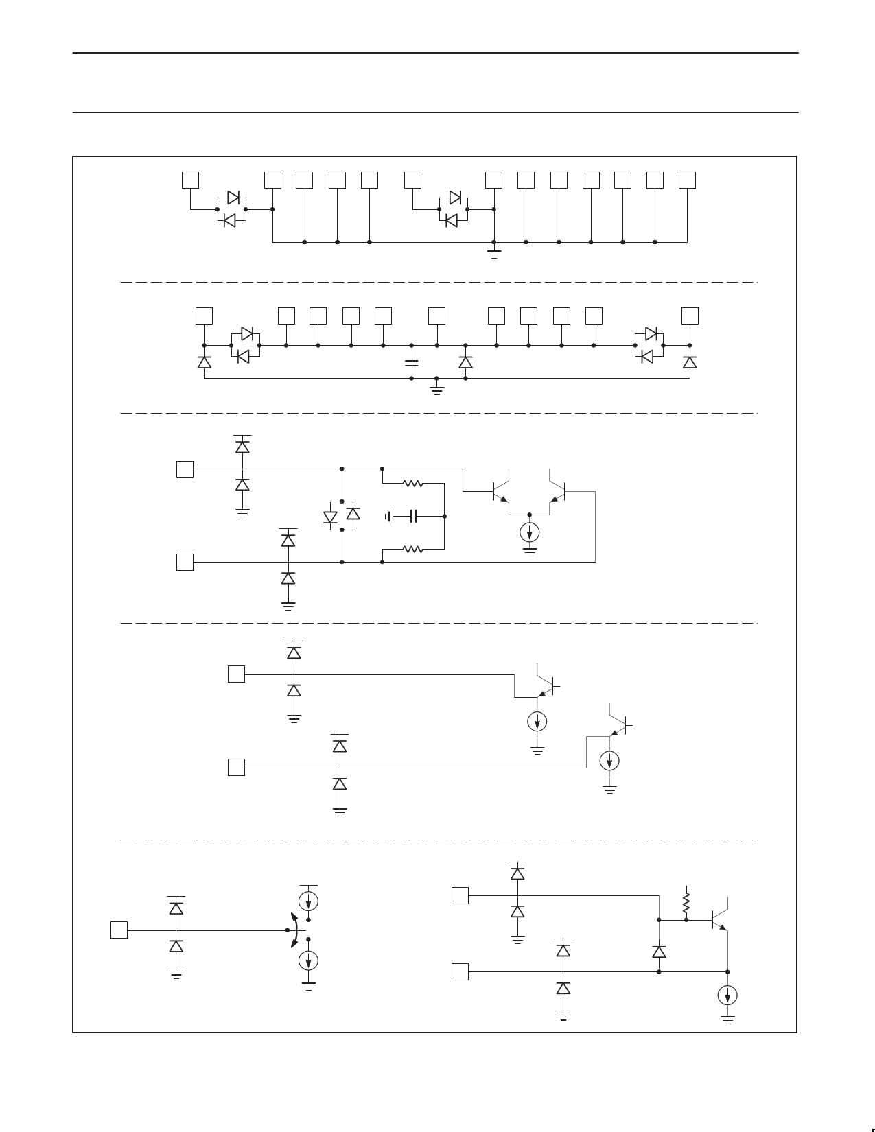
Figure 3. Pin Diagrams
5
SR00638
5 Page 
Philips Semiconductors
I/Q transmit modulator
Preliminary specification
SA900
control voltage from the VCO tank DC bias voltages. The VCO
tuning voltage is generated from the output of the PLL loop filter.
The VCO tank configuration is shown in Figure 6.
Crystal Oscillator (XO) Operation
For cellular radio applications, the SA900 will most likely utilize an
external reference TCXO in order to provide the frequency stability
necessary to operate to system requirements. The output of the
system TCXO can be AC coupled to the XTAL_1 input. However,
for applications that do not require such accuracy the XO circuit can
be configured as a Colpitts type oscillator with the addition of two
external capacitors along with the reference crystal and a trim
capacitor as shown in Figure 7.
Programmable Clock Outputs
The SA900 generates three buffered XO outputs used for external
reference signals. The XO feeds three sets of programmable
prescalers, the prescaler outputs are buffered to provide the CLK1,
CLK2 and MCLK signals. The CLK1 signal is a selectable divide 3/1
(X=1 divide 3, X=0 divide 1), 50% duty cycle, of the XO reference
signal. The CLK2 signal is a selectable divide 2/1 (Y=1 divide 2,
Y=0 divide 1), 50% duty cycle, of the XO reference signal. The
MCLK signal is a selectable divide 4/5/1 (CLKSET = VCC divide 4,
CLKSET = VCC/2 divide 5, and CLKSET = 0V divide 1), 50% duty
cycle, of the XO reference signal. MCLK is externally set by means
of the tri-level CLKSET input to provide a default master system
clock prior to programming the SA900.
Programming Operation
The SA900 is configured by means of a 3-wire input (CLOCK,
STROBE, DATA) to program the AMPS and DUAL modes, in
addition there are two power saving modes of operation, SLEEP and
STANDBY. The control logic section of the SA900 is designed using
low power CMOS logic. During SLEEP mode only the circuitry
required to provide a master clock (MCLK) to the digital portion of
the system is enabled. During the STANDBY mode of operation
MCLK, CLK1 and the TXLO and buffered LO outputs are powered
on, which may be the case when the system is in the receive only
mode. In the AMPS or DUAL operational modes all functions of the
SA900 are powered on to support receive, transmit and system
clock functions. The programming of the SA900 is identical to the
programming format of the SA7025 low-voltage 1GHz fractional-N
synthesizer, that can be used in conjunction with the SA900 to
provide the cellular radio channel selection.
The programming data is structured as a 24 bit long serial data
word; the word includes 4 address bits (dedicated 1 0 1 1) for chip
select. Data bits are shifted in on the leading edge of the clock, with
the least significant bit (LSB) first and the most significant bit (MSB)
last. Table 2 shows data word format, the 15th and last 5 bits are
not used. Figure 8 shows the chip timing diagram.
Address
A0 A1 A2 A3
10 1 1
Divide By N
N0 N1 Divide
00
10
01
6
7
8
11
9
AMPS/DUAL Mode
The A/D mode select enables or disables that portion of the circuitry
used for either the AMPS or DUAL mode of operation.
AD Mode
0 AMPS
1 DUAL
Synthesizer Enable
The SE bit turns on and off the synthesizer circuitry.
SE Operation
0 Disabled
1 Enabled
Sleep Mode 1
The SM1 bit is used to power down the TXLO buffer, the divide 3/1
prescaler and the CLK1 output buffer.
SM1
0
1
Operation
Power down
Power up (STANDBY)
Sleep Mode 2
The SM2 bit is used to power down the divide 2/1 prescaler and the
CLK2.
SM2
0
1
Operation
Power down
Power up (with
SM1=1 normal
operation)
Divide 3
X
0
1
Operation
Divide 1
Divide 3
Divide 2
Y
0
1
Operation
Divide 1
Divide 2
1997 Sept 16
11
11 Page | ||
| Páginas | Total 20 Páginas | |
| PDF Descargar | [ Datasheet SA900.PDF ] | |
Hoja de datos destacado
| Número de pieza | Descripción | Fabricantes |
| SA90 | 5.0 thru 170 volts 500 Watts Transient Voltage Suppressors | Microsemi Corporation |
| SA90 | 500W TRANSIENT VOLTAGE SUPPRESSORS | Won-Top Electronics |
| SA90 | TRANSZORB TRANSIENT VOLTAGE SUPPRESSOR | General Semiconductor |
| SA90 | GLASS PASSIVATED JUNCTION TRANSIENT VOLTAGE SUPPRESSOR(VOLTAGE - 5.0 TO 170 Volts 500 Watt Peak Pulse Power) | Pan Jit International Inc. |
| Número de pieza | Descripción | Fabricantes |
| SLA6805M | High Voltage 3 phase Motor Driver IC. |
Sanken |
| SDC1742 | 12- and 14-Bit Hybrid Synchro / Resolver-to-Digital Converters. |
Analog Devices |
|
DataSheet.es es una pagina web que funciona como un repositorio de manuales o hoja de datos de muchos de los productos más populares, |
| DataSheet.es | 2020 | Privacy Policy | Contacto | Buscar |
