|
|
|
PDF 74LVTH32244 Data sheet ( Hoja de datos )
| Número de pieza | 74LVTH32244 | |
| Descripción | Low Voltage 32-Bit Buffer/Line Driver with 3-STATE Outputs (Preliminary) | |
| Fabricantes | Fairchild Semiconductor | |
| Logotipo | ||
Hay una vista previa y un enlace de descarga de 74LVTH32244 (archivo pdf) en la parte inferior de esta página. Total 6 Páginas | ||
|
No Preview Available !
Preliminary
January 2001
Revised August 2001
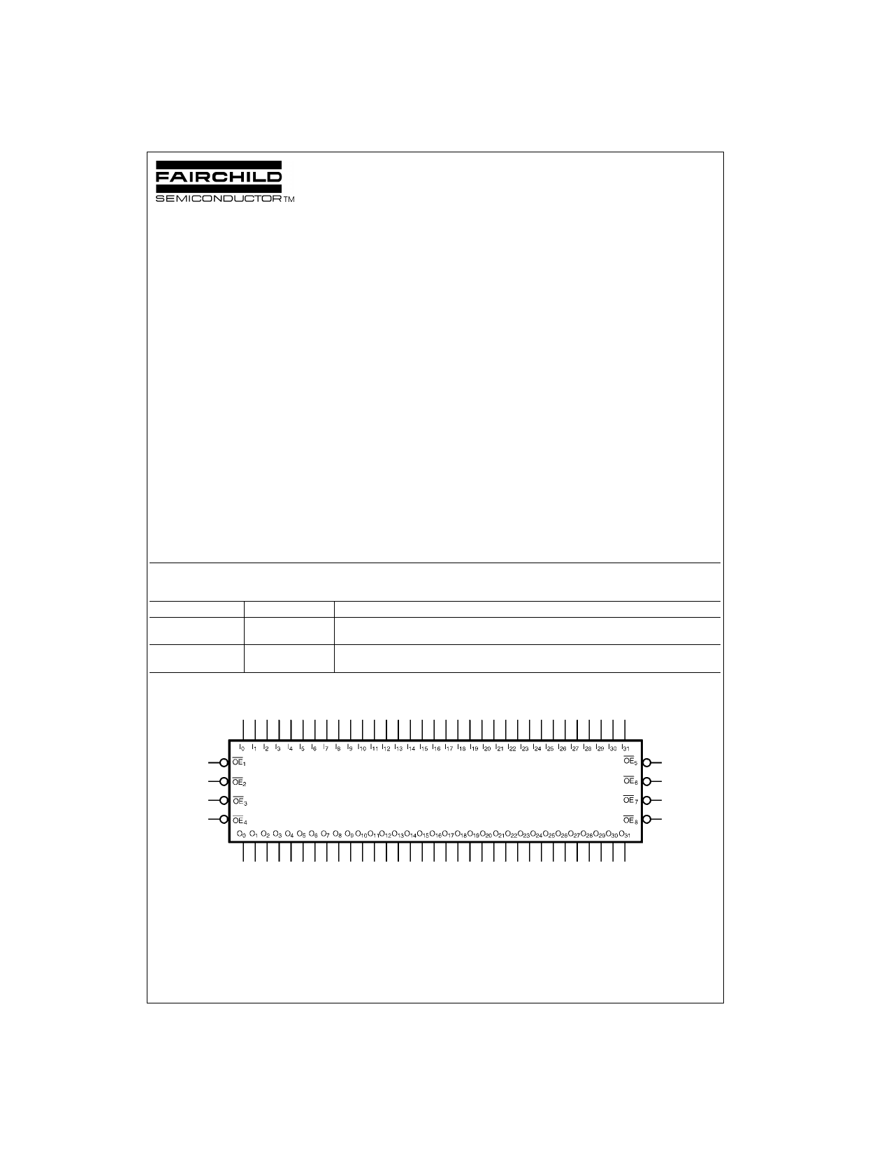
74LVT32244 • 74LVTH32244
Low Voltage 32-Bit Buffer/Line Driver
with 3-STATE Outputs (Preliminary)
General Description
The LVT32244 and LVTH32244 contain thirty-two non-
inverting buffers with 3-STATE outputs designed to be
employed as a memory and address driver, clock driver, or
bus oriented transmitter/receiver. The device is nibble con-
trolled. Individual 3-STATE control inputs can be shorted
together for 8-bit, 16-bit, or 32-bit operation.
The LVTH32244 data inputs include bushold, eliminating
the need for external pull-up resistors to hold unused
inputs.
These buffers and line drivers are designed for low-voltage
(3.3V) VCC applications, but with the capability to provide a
TTL interface to a 5V environment. The LVT32244 and
LVTH32244 are fabricated with an advanced BiCMOS
technology to achieve high speed operation similar to 5V
ABT while maintaining a low power dissipation
Features
s Input and output interface capability to systems at
5V VCC
s Bushold data inputs eliminate the need for external
pull-up resistors to hold unused inputs (74LVTH32244),
also available without bushold feature (74LVT32244).
s Live insertion/extraction permitted
s Power Up/Down high impedance provides glitch-free
bus loading
s Outputs source/sink −32 mA/+64 mA
s ESD performance:
Human-body model > 2000V
Machine model > 200V
Charged-device model > 1000V
s Packaged in plastic Fine-Pitch Ball Grid Array (FBGA)
(Preliminary)
Ordering Code:
Order Number Package Number
Package Description
74LVT32244GX
(Note 1)
BGA96A
96-Ball Fine-Pitch Ball Grid Array (FBGA), JEDEC MO-205, 5.5mm Wide
(Preliminary) [Tape and Reel]
74LVTH32244GX
(Note 1)
BGA96A
96-Ball Fine-Pitch Ball Grid Array (FBGA), JEDEC MO-205, 5.5mm Wide
(Preliminary) [Tape and Reel]
Note 1: BGA package available in Tape and Reel only.
Logic Symbol
© 2001 Fairchild Semiconductor Corporation DS500434
www.fairchildsemi.com
1 page 
DC Electrical Characteristics (Continued)
Preliminary
Symbol
Parameter
ICCH
ICCL
ICCZ
ICCZ+
Power Supply Current
Power Supply Current
Power Supply Current
Power Supply Current
VCC1 or VCC2
VCC1 or VCC2
VCC1 or VCC2
VCC1 or VCC2
VCC
(V)
3.6
3.6
3.6
3.6
TA = −40°C to +85°C
Min Max
0.19
5.0
0.19
0.19
Units
mA
mA
mA
mA
∆ICC
Increase in Power Supply Current
3.6
0.2 mA
(Note 7)
VCC1 or VCC2
Note 4: Applies to bushold versions only (LVTH32244).
Note 5: An external driver must source at least the specified current to switch from LOW-to-HIGH.
Note 6: An external driver must sink at least the specified current to switch from HIGH-to-LOW.
Note 7: This is the increase in supply current for each input that is at the specified voltage level rather than VCC or GND.
Conditions
Outputs High
Outputs Low
Outputs Disabled
VCC ≤ VO ≤ 5.5V,
Outputs Disabled
One Input at VCC − 0.6V
Other Inputs at VCC or GND
Dynamic Switching Characteristics (Note 8)
Symbol
Parameter
VCC TA = 25°C
(V) Min Typ Max
VOLP
Quiet Output Maximum Dynamic VOL
3.3
0.8
VOLV
Quiet Output Minimum Dynamic VOL
3.3
−0.8
Note 8: Characterized in SSOP package. Guaranteed parameter, but not tested.
Note 9: Max number of outputs defined as (n). n−1 data inputs are driven 0V to 3V. Output under test held LOW.
Units
V
V
Conditions
CL = 50 pF, RL = 500Ω
(Note 9)
(Note 9)
AC Electrical Characteristics
Symbol
Parameter
tPLH
tPHL
tPZH
tPZL
tPHZ
tPLZ
Propagation Delay Data to Output
Output Enable Time
Output Disable Time
TA = −40°C to +85°C
CL = 50 pF, RL = 500Ω
VCC = 3.3V ± 0.3V
VCC = 2.7V
Min Max Min Max
1.2 3.5 1.2 3.9
1.2 3.5 1.2 3.9
1.2 4.0 1.2 5.0
1.2 5.0 1.2 6.5
2.0 4.7 2.0 5.2
1.5 4.2 1.5 4.4
Capacitance (Note 10)
Symbol
Parameter
Conditions
CIN Input Capacitance
VCC = 0V, VI = 0V or VCC
COUT
Output Capacitance
VCC = 3.0V, VO = 0V or VCC
Note 10: Capacitance is measured at frequency f = 1 MHz, per MIL-STD-883, Method 3012.
Typical
4
8
Units
ns
ns
ns
Units
pF
pF
5 www.fairchildsemi.com
5 Page | ||
| Páginas | Total 6 Páginas | |
| PDF Descargar | [ Datasheet 74LVTH32244.PDF ] | |
Hoja de datos destacado
| Número de pieza | Descripción | Fabricantes |
| 74LVTH32244 | Low Voltage 32-Bit Buffer/Line Driver with 3-STATE Outputs (Preliminary) | Fairchild Semiconductor |
| 74LVTH32244GX | Low Voltage 32-Bit Buffer/Line Driver with 3-STATE Outputs (Preliminary) | Fairchild Semiconductor |
| 74LVTH32245 | Low Voltage 32-Bit Transceiver with 3-STATE Outputs | Fairchild Semiconductor |
| 74LVTH32245G | Low Voltage 32-Bit Transceiver with 3-STATE Outputs | Fairchild Semiconductor |
| Número de pieza | Descripción | Fabricantes |
| SLA6805M | High Voltage 3 phase Motor Driver IC. |
Sanken |
| SDC1742 | 12- and 14-Bit Hybrid Synchro / Resolver-to-Digital Converters. |
Analog Devices |
|
DataSheet.es es una pagina web que funciona como un repositorio de manuales o hoja de datos de muchos de los productos más populares, |
| DataSheet.es | 2020 | Privacy Policy | Contacto | Buscar |