|
|
|
PDF NAND01G-B Data sheet ( Hoja de datos )
| Número de pieza | NAND01G-B | |
| Descripción | (NAND0xG-B) NAND Flash Memory | |
| Fabricantes | ST Microelectronics | |
| Logotipo | ||
Hay una vista previa y un enlace de descarga de NAND01G-B (archivo pdf) en la parte inferior de esta página. Total 57 Páginas | ||
|
No Preview Available !
NAND01G-B, NAND02G-B,
NAND04G-B, NAND08G-B
1 Gbit, 2 Gbit, 4 Gbit, 8 Gbit
2112 Byte/1056 Word Page, 1.8V/3V, NAND Flash Memory
PRELIMINARY DATA
FEATURES SUMMARY
■ HIGH DENSITY NAND FLASH MEMORIES
– Up to 8 Gbit memory array
– Up to 64Mbit spare area
– Cost effective solutions for mass storage
applications
■ NAND INTERFACE
– x8 or x16 bus width
– Multiplexed Address/ Data
– Pinout compatibility for all densities
■ SUPPLY VOLTAGE
– 1.8V device: VDD = 1.7 to 1.95V
– 3.0V device: VDD = 2.7 to 3.6V
■ PAGE SIZE
– x8 device: (2048 + 64 spare) Bytes
– x16 device: (1024 + 32 spare) Words
■ BLOCK SIZE
– x8 device: (128K + 4K spare) Bytes
– x16 device: (64K + 2K spare) Words
■ PAGE READ / PROGRAM
– Random access: 25µs (max)
– Sequential access: 50ns (min)
– Page program time: 300µs (typ)
■ COPY BACK PROGRAM MODE
– Fast page copy without external buffering
■ CACHE PROGRAM AND CACHE READ
MODES
– Internal Cache Register to improve the
program and read throughputs
■ FAST BLOCK ERASE
– Block erase time: 2ms (typ)
■ STATUS REGISTER
■ ELECTRONIC SIGNATURE
■ CHIP ENABLE ‘DON’T CARE’
– for simple interface with microcontroller
■ SERIAL NUMBER OPTION
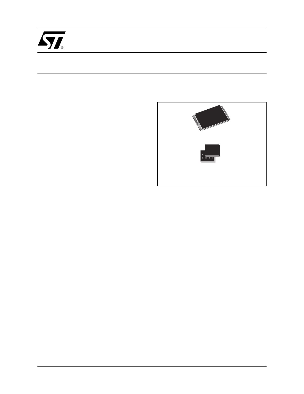
Figure 1. Packages
TSOP48 12 x 20mm
FBGA
VFBGA63 9.5 x 12 x 1mm
TFBGA63 9.5 x 12 x 1.2mm
■ DATA PROTECTION
– Hardware and Software Block Locking
– Hardware Program/Erase locked during
Power transitions
■ DATA INTEGRITY
– 100,000 Program/Erase cycles
– 10 years Data Retention
■ RoHS COMPLIANCE
– Lead-Free Components are Compliant
with the RoHS Directive
■ DEVELOPMENT TOOLS
– Error Correction Code software and
hardware models
– Bad Blocks Management and Wear
Leveling algorithms
– PC Demo board with simulation software
– File System OS Native reference software
– Hardware simulation models
October 2005
1/57
www.DataSheet4U.comThis is preliminary information on a new product now in development or undergoing evaluation. Details are subject to change without notice.
1 page 
NAND01G-B, NAND02G-B, NAND04G-B, NAND08G-B
Figure 18.Read Block Lock Status Operation . . . . . . . . . . . . . . . . . . . . . . . . . . . . . . . . . . . . . . . . . 33
Table 16. Block Lock Status . . . . . . . . . . . . . . . . . . . . . . . . . . . . . . . . . . . . . . . . . . . . . . . . . . . . . . 33
Figure 19.Block Protection State Diagram . . . . . . . . . . . . . . . . . . . . . . . . . . . . . . . . . . . . . . . . . . . 34
SOFTWARE ALGORITHMS . . . . . . . . . . . . . . . . . . . . . . . . . . . . . . . . . . . . . . . . . . . . . . . . . . . . . . . . . 35
Bad Block Management . . . . . . . . . . . . . . . . . . . . . . . . . . . . . . . . . . . . . . . . . . . . . . . . . . . . . . . . 35
Block Replacement . . . . . . . . . . . . . . . . . . . . . . . . . . . . . . . . . . . . . . . . . . . . . . . . . . . . . . . . . . . . 35
Table 17. Block Failure . . . . . . . . . . . . . . . . . . . . . . . . . . . . . . . . . . . . . . . . . . . . . . . . . . . . . . . . . . 35
Figure 20.Bad Block Management Flowchart . . . . . . . . . . . . . . . . . . . . . . . . . . . . . . . . . . . . . . . . . 35
Figure 21.Garbage Collection . . . . . . . . . . . . . . . . . . . . . . . . . . . . . . . . . . . . . . . . . . . . . . . . . . . . . 36
Garbage Collection . . . . . . . . . . . . . . . . . . . . . . . . . . . . . . . . . . . . . . . . . . . . . . . . . . . . . . . . . . . . 36
Wear-leveling Algorithm . . . . . . . . . . . . . . . . . . . . . . . . . . . . . . . . . . . . . . . . . . . . . . . . . . . . . . . . 36
Error Correction Code. . . . . . . . . . . . . . . . . . . . . . . . . . . . . . . . . . . . . . . . . . . . . . . . . . . . . . . . . . 36
Figure 22.Error Detection . . . . . . . . . . . . . . . . . . . . . . . . . . . . . . . . . . . . . . . . . . . . . . . . . . . . . . . . 36
Hardware Simulation Models . . . . . . . . . . . . . . . . . . . . . . . . . . . . . . . . . . . . . . . . . . . . . . . . . . . . 37
Behavioral simulation models . . . . . . . . . . . . . . . . . . . . . . . . . . . . . . . . . . . . . . . . . . . . . . . . . . . . . 37
IBIS simulations models . . . . . . . . . . . . . . . . . . . . . . . . . . . . . . . . . . . . . . . . . . . . . . . . . . . . . . . . . 37
PROGRAM AND ERASE TIMES AND ENDURANCE CYCLES . . . . . . . . . . . . . . . . . . . . . . . . . . . . . 38
Table 18. Program, Erase Times and Program Erase Endurance Cycles . . . . . . . . . . . . . . . . . . . 38
MAXIMUM RATING. . . . . . . . . . . . . . . . . . . . . . . . . . . . . . . . . . . . . . . . . . . . . . . . . . . . . . . . . . . . . . . . 38
Table 19. Absolute Maximum Ratings . . . . . . . . . . . . . . . . . . . . . . . . . . . . . . . . . . . . . . . . . . . . . . . 38
DC AND AC PARAMETERS. . . . . . . . . . . . . . . . . . . . . . . . . . . . . . . . . . . . . . . . . . . . . . . . . . . . . . . . . 39
Table 20. Operating and AC Measurement Conditions . . . . . . . . . . . . . . . . . . . . . . . . . . . . . . . . . . 39
Table 21. Capacitance . . . . . . . . . . . . . . . . . . . . . . . . . . . . . . . . . . . . . . . . . . . . . . . . . . . . . . . . . . 39
Table 22. DC Characteristics, 1.8V Devices . . . . . . . . . . . . . . . . . . . . . . . . . . . . . . . . . . . . . . . . . . 39
Figure 23.Equivalent Testing Circuit for AC Characteristics Measurement. . . . . . . . . . . . . . . . . . . 40
Table 23. DC Characteristics, 3V Devices. . . . . . . . . . . . . . . . . . . . . . . . . . . . . . . . . . . . . . . . . . . . 41
Table 24. AC Characteristics for Command, Address, Data Input . . . . . . . . . . . . . . . . . . . . . . . . . 42
Table 25. AC Characteristics for Operations . . . . . . . . . . . . . . . . . . . . . . . . . . . . . . . . . . . . . . . . . . 43
Figure 24.Command Latch AC Waveforms . . . . . . . . . . . . . . . . . . . . . . . . . . . . . . . . . . . . . . . . . . . 44
Figure 25.Address Latch AC Waveforms . . . . . . . . . . . . . . . . . . . . . . . . . . . . . . . . . . . . . . . . . . . . 44
Figure 26.Data Input Latch AC Waveforms . . . . . . . . . . . . . . . . . . . . . . . . . . . . . . . . . . . . . . . . . . . 45
Figure 27.Sequential Data Output after Read AC Waveforms . . . . . . . . . . . . . . . . . . . . . . . . . . . . 45
Figure 28.Read Status Register AC Waveform . . . . . . . . . . . . . . . . . . . . . . . . . . . . . . . . . . . . . . . . 46
Figure 29.Read Electronic Signature AC Waveform . . . . . . . . . . . . . . . . . . . . . . . . . . . . . . . . . . . . 46
Figure 30.Page Read Operation AC Waveform . . . . . . . . . . . . . . . . . . . . . . . . . . . . . . . . . . . . . . . 47
Figure 31.Page Program AC Waveform . . . . . . . . . . . . . . . . . . . . . . . . . . . . . . . . . . . . . . . . . . . . . 48
Figure 32.Block Erase AC Waveform . . . . . . . . . . . . . . . . . . . . . . . . . . . . . . . . . . . . . . . . . . . . . . . 49
Figure 33.Reset AC Waveform . . . . . . . . . . . . . . . . . . . . . . . . . . . . . . . . . . . . . . . . . . . . . . . . . . . . 49
Ready/Busy Signal Electrical Characteristics . . . . . . . . . . . . . . . . . . . . . . . . . . . . . . . . . . . . . . 50
Figure 34.Ready/Busy AC Waveform . . . . . . . . . . . . . . . . . . . . . . . . . . . . . . . . . . . . . . . . . . . . . . . 50
Figure 35.Ready/Busy Load Circuit. . . . . . . . . . . . . . . . . . . . . . . . . . . . . . . . . . . . . . . . . . . . . . . . . 50
Figure 36.Resistor Value Versus Waveform Timings For Ready/Busy Signal . . . . . . . . . . . . . . . . 50
5/57
5 Page 
NAND01G-B, NAND02G-B, NAND04G-B, NAND08G-B
Figure 5. FBGA63 Connections, x8 devices (Top view through package)
12 3
4 5 6 7 8 9 10
A DU DU
DU DU
B DU
DU DU
C
WP AL VSS E
W RB
D NC R CL NC NC NC
E NC NC NC NC NC NC
F NC NC NC NC NC NC
G NC NC NC NC NC PRL
H NC I/O0 NC NC NC VDD
J NC I/O1 NC VDD I/O5 I/O7
K VSS I/O2 I/O3 I/O4 I/O6 VSS
L DU DU
DU DU
M DU DU
DU DU
AI09376
11/57
11 Page | ||
| Páginas | Total 57 Páginas | |
| PDF Descargar | [ Datasheet NAND01G-B.PDF ] | |
Hoja de datos destacado
| Número de pieza | Descripción | Fabricantes |
| NAND01G-A | 128 Mbit / 256 Mbit / 512 Mbit / 1 Gbit (x8/x16) 528 Byte/264 Word Page / 1.8V/3V / NAND Flash Memories | STMicroelectronics |
| NAND01G-B | (NAND0xG-B) NAND Flash Memory | ST Microelectronics |
| NAND01G-B2B | (NAND0xG-B2x) NAND Flash Memory | ST Microelectronics |
| NAND01G-B2B | NAND flash memory | Numonyx |
| Número de pieza | Descripción | Fabricantes |
| SLA6805M | High Voltage 3 phase Motor Driver IC. |
Sanken |
| SDC1742 | 12- and 14-Bit Hybrid Synchro / Resolver-to-Digital Converters. |
Analog Devices |
|
DataSheet.es es una pagina web que funciona como un repositorio de manuales o hoja de datos de muchos de los productos más populares, |
| DataSheet.es | 2020 | Privacy Policy | Contacto | Buscar |