|
|
|
PDF CLA200 Data sheet ( Hoja de datos )
| Número de pieza | CLA200 | |
| Descripción | CMOS Gate Arrays | |
| Fabricantes | Zarlink Semiconductor | |
| Logotipo | ||
Hay una vista previa y un enlace de descarga de CLA200 (archivo pdf) en la parte inferior de esta página. Total 11 Páginas | ||
|
No Preview Available !
( DataSheet : www.DataSheet4U.com )
CLA200 Series
CMOS Gate Arrays
Advance Information
INTRODUCTION
The CLA200 Series Arrays from Zarlink Semiconductor offer
designers the capability to integrate designs of more than 2
million gates. There are 14 fixed arrays optimised for low to
medium complexity designs ranging from 11K used gates up
to 628K used gates. For larger designs optimised arrays can
be built with up to 3 million available gates. Using automated
gate array base constructor software, a tailor made optimised
gate array can be built to customers requirements which gives
designers the ability to specify the optimum die size whilst
retaining the benefits of standard gate arrays. Utilising a gate
array architecture allows the base arrays to be pre-
manufactured enabling gate array prototype lead time to be
offered.
Supported with high quality design kits for a range of industry
standard CAE tools, the CLA200 Series provide customers
with a low risk, low cost solution and fast time to market.
FEATURES
• 0.35µm drawn Channel Length
• Three (CLT) and Four (CLQ) layer metal options
• Automated base array constructor for optimised arrays
with up to 3 million gates
• Low Power, 0.4µW/MHz/Gate at 3V (2-input NAND with
two loads)
• 135ps gate delay for 2-input NAND with two loads (3V)
• High density staggered pad ring
• Wide range of package options including QFP & BGA
• Characterised for operation from 1.8V to 3.6V
• 2V and 3.3V I/O capability on the same device
• 5V tolerant inputs, outputs and bidirectionals
• Accurate delay modelling for gates and tracks with sign
off quality CAE design libraries for QuickSim II and
Verilog-XL
• VITAL Sign off with Synopsys VSS Simulator
• CAD libraries optimised for synthesis
• Methodologies for low clock skew
• Full set of I/O cells for direct pad synthesis
• Variable output slew rates for low noise
• IDDQ Testing
BENEFITS
• Fast Customer Time To Market
- Direct sign-off on Industry Standard CAE tools
- Comprehensive Industry Standard CAE tools
- SystemBuilder™ megacell libraries
- World-wide design center support
- Reliable prototype and production delivery
- Dual silicon sources
DS4812
ISSUE 1.3
July 1997
• Cost -effective solutions
- Optimised silicon architecture for high density silicon
utilisation
- ISO9001 Factory with Statistical process control for
optimum yield
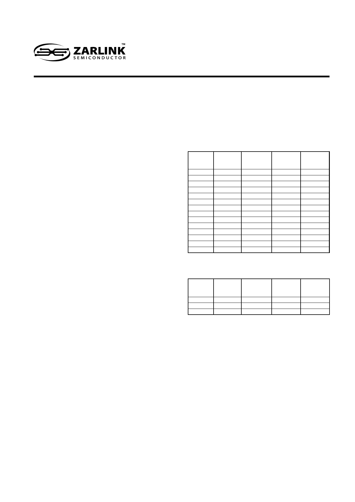
FIXED ARRAY SIZES
Available Available
Pads
Gates
CLA201
CLA202
CLA203
CLA204
CLA205
CLA206
CLA207
CLA208
CLA209
CLA210
CLA211
CLA212
CLA213
CLA214
48
64
80
100
128
144
160
176
208
240
272
304
328
352
17,860
30,012
45,300
68,736
109,980
137,812
168,780
202,884
280,500
370,660
473,364
588,612
683,280
785,004
Usable
Gates
TLM
10,700
18,000
27,200
41,200
66,000
82,700
101,300
121,700
168,300
222,400
284,000
353,200
410,000
471,000
Usable
Gates
QLM
14,300
24,000
36,200
55,000
88,000
110,200
135,000
162,300
224,400
296,500
378,700
470,900
546,600
628,000
OPTIMISED ARRAYS
The following table illustrates examples of possible compiled
array sizes.
Available Available
Pads
Gates
Usable
Gates
TLM
Usable
Gates
QLM
CLA2xx
400
989,740 590,000
790,000
CLA2xx
552
1,879,776 1,100,000 1,500,000
CLA2xx
700
3,018,424 1,800,000 2,400,000
www.DataSheet4U.com
www.DataSheet4U.com
1 page 
Stage 1
Stage 2
Stage 3
Figure.1
Advance Information CLA200 Series
Advanced Delay Modelling
Delay calculation includes the following features:
• Edge speed modelling
• Pin to pin timings
• Non-linear delay modelling
• Accurate delay derating
• Conditional delay modelling
Pin to Pin Delays
Delay models use times between individual input and output
pins for both rising and falling delays, as illustrated in figure 3
below.
Stage 1 output grid
Stage 2 output grid
Stage 3 output grid
Figure.2
A
BF
C
Figure.3
Calculation uses individual pin to pin delays, e.g. A to F and B
to F, which improves simulation accuracy by modelling the
considerable variation in delay between different input pins.
For complex gates (e.g. AND-NOR gates or adders) the
variation is up to 40%. For simple NAND and NOR logic gates
the typical variation is 20%.
Non-linear Curve Fitting
For fast input edges (0.5ns) delay time increases linearly with
the output load, whereas for high output loads delay increases
linearly with edge speed. Delays for slow input edges and light
input loads do not follow the linear model, so a simple linear
model cannot represent delays accurately. A more complex
equation, which includes interaction between edge and load
factors, is used to model delays.
Thermal Management
The increase in speed and density available through
advanced CMOS processes results in a corresponding
increase in power dissipation. Designs can now have more
than half a million used gates and chip power consumption is
an important issue.
The CLA200 series offers the following:
• Lower power CMOS for improved thermal management
• Software constructed power grids for efficient power
distribution
• Copper lead frame QFPs for lower thermal resistance
• High pinout power packages available
5
5 Page 
http://www.zarlink.com
World Headquarters - Canada
Tel: +1 (613) 592 0200
Fax: +1 (613) 592 1010
North America - West Coast
Tel: (858) 675-3400
Fax: (858) 675-3450
North America - East Coast
Tel: (978) 322-4800
Fax: (978) 322-4888
Asia/Pacific
Tel: +65 333 6193
Fax: +65 333 6192
Europe, Middle East,
and Africa (EMEA)
Tel: +44 (0) 1793 518528
Fax: +44 (0) 1793 518581
Information relating to products and services furnished herein by Zarlink Semiconductor Inc. trading as Zarlink Semiconductor or its subsidiaries (collectively “Zarlink”) is
believed to be reliable. However, Zarlink assumes no liability for errors that may appear in this publication, or for liability otherwise arising from the application or use of any
such information, product or service or for any infringement of patents or other intellectual property rights owned by third parties which may result from such application or
use. Neither the supply of such information or purchase of product or service conveys any license, either express or implied, under patents or other intellectual property rights
owned by Zarlink or licensed from third parties by Zarlink, whatsoever. Purchasers of products are also hereby notified that the use of product in certain ways or in
combination with Zarlink, or non-Zarlink furnished goods or services may infringe patents or other intellectual property rights owned by Zarlink.
This publication is issued to provide information only and (unless agreed by Zarlink in writing) may not be used, applied or reproduced for any purpose nor form part of any
order or contract nor to be regarded as a representation relating to the products or services concerned. The products, their specifications, services and other information
appearing in this publication are subject to change by Zarlink without notice. No warranty or guarantee express or implied is made regarding the capability, performance or
suitability of any product or service. Information concerning possible methods of use is provided as a guide only and does not constitute any guarantee that such methods of
use will be satisfactory in a specific piece of equipment. It is the user’s responsibility to fully determine the performance and suitability of any equipment using such
information and to ensure that any publication or data used is up to date and has not been superseded. Manufacturing does not necessarily include testing of all functions or
parameters. These products are not suitable for use in any medical products whose failure to perform may result in significant injury or death to the user. All products and
materials are sold and services provided subject to Zarlink Semiconductor’s conditions of sale which are available on request.
Purchase of Zarlink’s I2C components conveys a licence under the Philips I2C Patent rights to use these components in an I2C System, provided that the system conforms
to the I2C Standard Specification as defined by Philips
Zarlink and the Zarlink Semiconductor logo are trademarks of Zarlink Semiconductor Inc.
Copyright 2001, Zarlink Semiconductor Inc. All rights reserved.
TECHNICAL DOCUMENTATION - NOT FOR RESALE
11 Page | ||
| Páginas | Total 11 Páginas | |
| PDF Descargar | [ Datasheet CLA200.PDF ] | |
Hoja de datos destacado
| Número de pieza | Descripción | Fabricantes |
| CLA200 | CMOS Gate Arrays | Zarlink Semiconductor |
| Número de pieza | Descripción | Fabricantes |
| SLA6805M | High Voltage 3 phase Motor Driver IC. |
Sanken |
| SDC1742 | 12- and 14-Bit Hybrid Synchro / Resolver-to-Digital Converters. |
Analog Devices |
|
DataSheet.es es una pagina web que funciona como un repositorio de manuales o hoja de datos de muchos de los productos más populares, |
| DataSheet.es | 2020 | Privacy Policy | Contacto | Buscar |