|
|
|
PDF CLA60000 Data sheet ( Hoja de datos )
| Número de pieza | CLA60000 | |
| Descripción | Channel Less CMOS Gate Arrays | |
| Fabricantes | Zarlink Semiconductor | |
| Logotipo | ||
Hay una vista previa y un enlace de descarga de CLA60000 (archivo pdf) en la parte inferior de esta página. Total 15 Páginas | ||
|
No Preview Available !
( DataSheet : www.DataSheet4U.com )
CLA60000 Series
Channel less CMOS Gate Arrays
This new family of gate arrays uses many innovative
techniques to achieve 110K gates per chip with
system clock speeds of up to 70MHz. The
combination of high speed, high gate complexity and
low power operation places Zarlink Semiconductor
at the forefront of ASIC capability.
General Description
The CLA60000 gate array family is Zarlink
Semiconductor’s fifth-generation CMOS gate array
product. These arrays allow even higher integration
densities at enhanced system clock rates as need for
many of today’s system applications.
The largest array in the family at 110K gates offers a
tenfold increase in raw gate availability then
channelled gate arrays. In addition, many new
designs features have been incorporated such as
analog functionality, slew rate output control, and
intermediate I/O buffering for optimum data transfer
through peripheral cells.
Also, the low-power characteristics of Zarlink
Semiconductor CMOS processing have been
incorporated in these arrays, easing the thermal
management problems associated with complex
designs of 20,000 gates and above.
Features
• Channel less arrays to 110,000 gates
• 1.4 micron dual layer metal silicon CMOS
process
• Typical Gate Delays of 700ps (NAND2)
• Comprehensive cell library including microcells,
macrocells, and paracells
• Power distribution optimized for maximum noise
immunity
• Slew controlled outputs with up to 24mA drivers
• Fully supported by design software (PDS2) and
popular workstations
• Very high latch up immunity
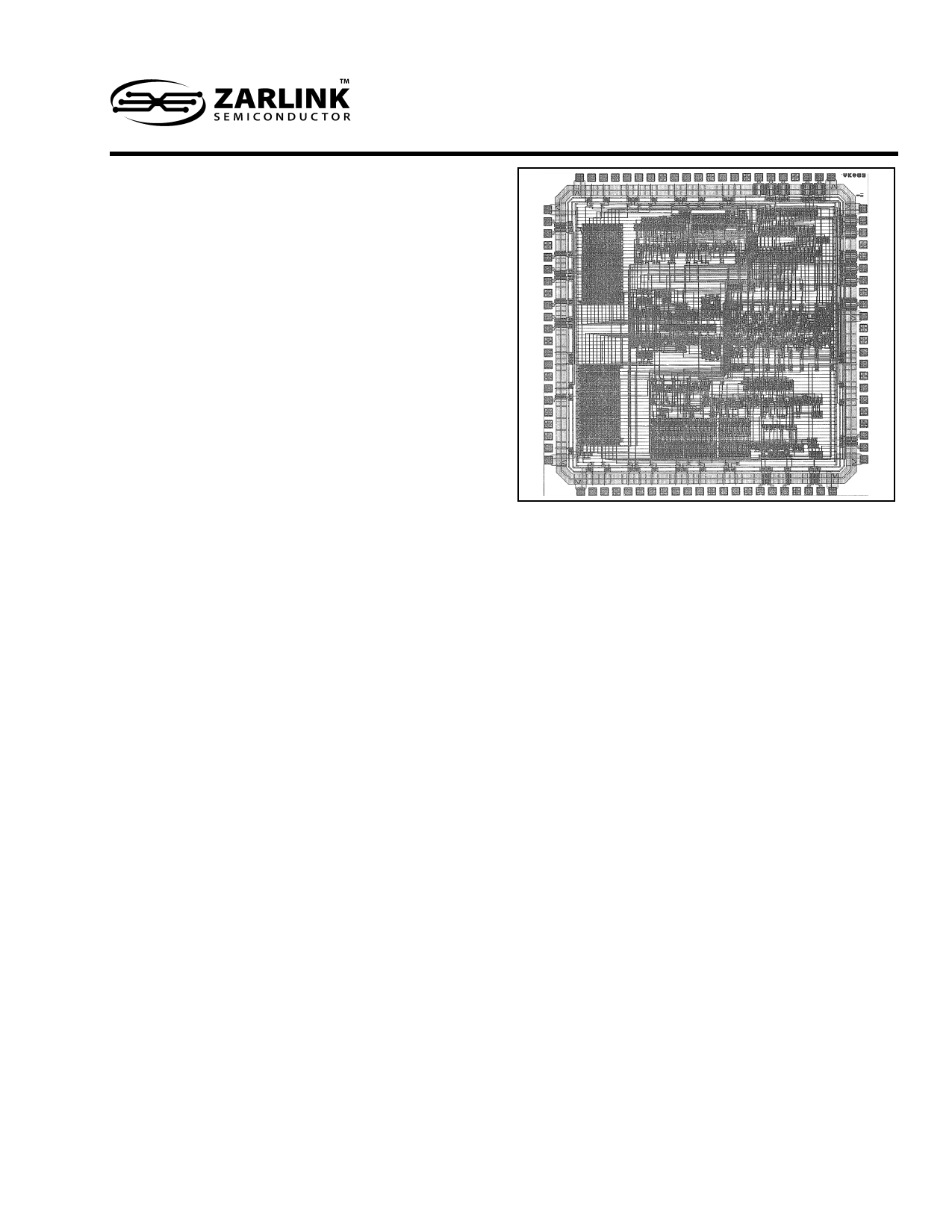
Figure 1 - CLA60000 Chip Microplot
All CLA60000 arrays have the same construction. A
core of uncommitted transistors is arranged for
optimum connection as logic functions and
surrounded by uncommitted peripheral (I/O) circuitry.
The channel less array architecture is an important
feature - the absence of discrete wiring channels
increases flexibility, reduces track capacitance whilst
significantly increasing transistor sizes for improved
logic performance.
The construction of the basic building blocks have
been planned to support basic logic functions, macro
functions, and core memory functions (RAM and
ROM) with high routability. Logic programmability is
given by dual level metal, with interconnecting vias,
plus a forth level of programmability (contacts).
The overall architecture of these gate arrays has
been designed to exploit many new and emerging
developments in CAD tools. Increasing demands are
now being made for design tools which are faster,
easier to use, and more accurate. The Zarlink
Semiconductor Design System (PDS2) allows full
control over all aspects of design including logic
capture, simulation and layout.
www.DataSheet4U.com
1
www.DataSheet4U.com
1 page 
CLA60000 Series
Design Thermal Management
As gate integration capacity improves with CMOS
process geometry reduction, the ability of silicon to
exceed the power capabilities of accepted packaging
technology is a very real problem. Semi-Custom
designers now have the ability to design circuits of
50,000 gates and over, and chip power consumption
is (or should be) a very important concern.
With complexities approaching 100K gates, the core
power at gate level becomes increasingly more
dominant. It becomes essential to offer ultra low
power core logic to maintain an acceptable overall
chip power budget (typically 1 Watt for standard
surface mount packaging).
The consequences of higher power consumption are
elevated chip temperatures and reductions in
product reliability, otherwise relatively expensive
special packaging has to be considered which is
bulkier and more costly.
Zarlink Semiconductor’s CLA60000 arrays offer low
power factors. At 5mW per gate per MHz gate power
and 2mW per gate load, power is lower than most
competitive arrays, with lower operating
temperatures and higher inherent long term
reliability.
CLA60000 Power Dissipation Calculation
CLA60000 series power dissipation for any array can be estimated by following this example (calculated for the
CLA68XXX).
Number of available gates
Percent gates used
Number of used gates
Number of gates switching each
clock cycle (15%)
Power dissipation/gate/MHz (µW)
(gate fanout typically 2 loads)
Total core dissipation/MHz (mW)
Number of available I/O pads
Percent of I/O pads used as Outputs
Number of I/O pads used as Outputs
Number of output buffers switching
each clock cycle (20%)
110112
40%
44045
6607
9
59.5
280
40
112
22
Dissipation/output buffers/MHz/pF (µW) 25
Output loading in pF
50
Power/output buffer/MHz (mW)
1.25
Total output buffer dissipation/MHz (mW) 27.5
Total Power dissipation/MHz (mW)
87
Total Power at 10MHz clock rate (W)
Total Power at 25MHz clock rate (W)
0.87
2.18
1.4 Micron CMOS Process
The 1.4 micron CMOS process Zarlink Semiconductor process variant VJ) uses the latest manufacturing
techniques at Zarlink Semiconductor’s Class 1, 6-inch fabrication facility in Roborough, England. The process
can be described as a twin well, self aligned LOCOS isolated technology on an epitaxial substrate giving low
defect density and high reliability.
Effective channel length is 1.1 micron. Usable gate packaging density is 600 gates/sq.mm on two levels of
metal. Devices will operate up to a maximum junction temperature of 170 Deg.C, and show excellent
hardness, ESD, and stable performance.
ABSOLUTE MAXIMUM RATINGS
PARAMETER
MIN
MAX
UNITS
Supply Voltage
-0.5 7.0
V
Input Voltage
-0.5 Vdd+0.5
V
Output Voltage
-0.5 Vdd+0.5
V
Storage Temperature:
Ceramic
-65 150 Deg.C
Plastic
-40 125 Deg.C
Operation above these absolute maximum ratings may
permanently damage device characteristics and may affect
reliability.
RECOMMENDED OPERATING LIMITS
PARAMETER
MIN
MAX
UNITS
Supply Voltage
3.0 6.0
V
Input Voltage
Vss Vdd
V
Output Voltage
Vss Vdd
V
Current per pad
100 mA
Operating Temperature:
Commercial Grade
0 70 Deg.C
Industrial Grade
-40 85 Deg.C
Military Grade
-55 125 Deg.C
5
5 Page 
CLA60000 Series
CLKA
2CLKA
CLKAP
CLKAM
CLKB
DRV3
DRV6
Basic Clock Driver
Dual Basic Clock Driver
Basic Clock Driver + Inverter
Basic Clock Driver + Inverter
Large Clock Driver + Inverter
Triple Output Internal Driver
Hex Output Internal Driver
TM
2TM
BDR
Buffered Transmission Gate
Transmission Gate for 2 to 1
Multiplexing
Bus Driver
DL
DL2
DLRS
DLARS
DF
DFRS
MDF
MDFRS
M3DF
M3DFRS
JK
JKRS
JBARK
JBARKRS
BDL
BDLRS
BDLARS
BDF
BDFRS
BMDF
BMDFRS
TRID
Data Latch
Data Latch
Data Latch with Set and Reset
Data Latch with Set and Reset
Master-Slave D-Type Flip-Flop
Master-Slave D-Type Flip-Flop with Set
and Reset
Multiplexed Master-Slave D-Type Flip-
Flop
Multiplexed Master-Slave D-Type Flip-
Flop with Set and Reset
3 to 1 Multiplexed Master-Slave D-Type
Flip-Flop
3 to 1 Multiplexed Master-Slave D-Type
Flip-Flop with Set and Reset
J K Flip-Flop
J K Flip-FLop with Set and Reset
J K Flip-Flop
J K Flip-Flop with Set and Reset
Buffered Data Latch
Buffered Data Latch with Set and Reset
Buffered Data Latch with Set and Reset
Buffered Master-Slave D-Type Flip-Flop
Buffered Master-Slave D-Type Flip-Flop
with Set and Reset
Buffered Multiplexed Master-Slave D-
Type Flip-Flop
Buffered Multiplexed Master-Slave D-
Type Flip-Flop with Set and Reset
Tri-State Driver
Intermediate Buffers:
IBST1
IBST2
IBSK1
IBSK2
IBSK3
IBTRID
Input Buffer with CMOS switching level
Input Buffer with 2V switching level
Driver with Lightly Skewed Outputs
Driver with Medium Skewed Outputs
Driver with Heavily Skewed Outputs
Tri-State Driver
IBTRID1
IBTRID2
IBTRID3
IBGATE
IB2D
IBCLKB
IBDF
IBDFA
IBCMOS1
IBCMOS2
IBTTL1
IBTTL2
Tri-State Driver with Lightly Skewed
Outputs + 2 Inverters
Tri-State Driver with Medium Skewed
Outputs + 2 Inverters
Tri-State Driver with Heavily Skewed
Outputs + 2 Inverters
Large 2-Input NAND Gate + Large 2-
Input NOR Gate
Dual High Power Inverters
Large Clock Driver
Master-Slave D-Type Flip-Flop
Master-Slave D-Type Flip-Flop
CMOS Input Buffer and Large 2-Input
NAND Gate
CMOS Input Buffer and Data Latch
TTL Input Buffer and Large 2-Input
NAND Gate
TTL Input Buffer and Data Latch
Input Buffer:
IPNR
IPR1P
IPR1M
IPR2P
IPR2M
IPR3P
IPR3M
IPR4P
IPR4M
Input Cell (with no Pullup or Pulldown
resistors)
Input Cell with 1K-Ohm Pull-up Resistor
Input Cell with 1K-Ohm Pull-down
Resistor
Input Cell with 2K-Ohm Pull-up Resistor
Input Cell with 2K-Ohm Pull-down
Resistor
Input Cell with 4K-Ohm Pull-up Resistor
Input Cell with 4K-Ohm Pull-down
Resistor
Input Cell with 100K-Ohm Pull-up
Resistor
Input Cell with 100K-Ohm Pull-down
Resistor
Output Buffers:
OP1
OP2
OP3
OP6
OP12
Smallest Drive Output Buffer
Small Drive Output Buffer
Standard Drive Output Buffer
Medium Drive Output Buffer
Large Drive Output Buffer
OP5B
OP11B
Standard Drive Non-Inverting Output
Buffer
Large Drive Non-Inverting Output Buffer
OPT1
OPT2
OPT3
OPT6
Smallest Drive Tri-State Output Buffer
Small Drive Tri-State Output Buffer
Standard Drive Tri-State Output Buffer
Medium Drive Tri-State Output Buffer
11
11 Page | ||
| Páginas | Total 15 Páginas | |
| PDF Descargar | [ Datasheet CLA60000.PDF ] | |
Hoja de datos destacado
| Número de pieza | Descripción | Fabricantes |
| CLA60000 | Channel Less CMOS Gate Arrays | Zarlink Semiconductor |
| Número de pieza | Descripción | Fabricantes |
| SLA6805M | High Voltage 3 phase Motor Driver IC. |
Sanken |
| SDC1742 | 12- and 14-Bit Hybrid Synchro / Resolver-to-Digital Converters. |
Analog Devices |
|
DataSheet.es es una pagina web que funciona como un repositorio de manuales o hoja de datos de muchos de los productos más populares, |
| DataSheet.es | 2020 | Privacy Policy | Contacto | Buscar |