|
|
PDF HD6472394 Data sheet ( Hoja de datos )
| Número de pieza | HD6472394 | |
| Descripción | (HD6472357 Series) 16-Bit Microcomputer | |
| Fabricantes | Renesas | |
| Logotipo |  |
|
Hay una vista previa y un enlace de descarga de HD6472394 (archivo pdf) en la parte inferior de esta página. Total 30 Páginas | ||
|
No Preview Available !
www.DataSheet4U.com
To all our customers
Regarding the change of names mentioned in the document, such as Hitachi
Electric and Hitachi XX, to Renesas Technology Corp.
The semiconductor operations of Mitsubishi Electric and Hitachi were transferred to Renesas
Technology Corporation on April 1st 2003. These operations include microcomputer, logic, analog
and discrete devices, and memory chips other than DRAMs (flash memory, SRAMs etc.)
Accordingly, although Hitachi, Hitachi, Ltd., Hitachi Semiconductors, and other Hitachi brand
names are mentioned in the document, these names have in fact all been changed to Renesas
Technology Corp. Thank you for your understanding. Except for our corporate trademark, logo and
corporate statement, no changes whatsoever have been made to the contents of the document, and
these changes do not constitute any alteration to the contents of the document itself.
Renesas Technology Home Page: http://www.renesas.com
www.DataSheet4U.com
Renesas Technology Corp.
Customer Support Dept.
April 1, 2003
www.DataSheet4U.com
1 page 
www.DataSheet4U.com
General Precautions on Handling of Product
1. Treatment of NC Pins
Note: Do not connect anything to the NC pins.
The NC (not connected) pins are either not connected to any of the internal circuitry or are they
are used as test pins or to reduce noise. If something is connected to the NC pins, the operation
of the LSI is not guaranteed.
2. Treatment of Unused Input Pins
Note: Fix all unused input pins to high or low level.
Generally, the input pins of CMOS products are high-impedance input pins. If unused pins are
in their open states, intermediate levels are induced by noise in the vicinity, a pass-through
current flows internally, and a malfunction may occur.
3. Processing before Initialization
Note: When power is first supplied, the product’s state is undefined.
The states of internal circuits are undefined until full power is supplied throughout the chip and
a low level is input on the reset pin. During the period where the states are undefined, the
register settings and the output state of each pin are also undefined. Design your system so
that it does not malfunction because of processing while it is in this undefined state. For those
products which have a reset function, reset the LSI immediately after the power supply has
been turned on.
4. Prohibition of Access to Undefined or Reserved Addresses
www.DataSheet4U.comNote: Access to undefined or reserved addresses is prohibited.
The undefined or reserved addresses may be used to expand functions, or test registers may
have been be allocated to these addresses. Do not access these registers; the system’s
operation is not guaranteed if they are accessed.
www.DataSheet4U.com
5 Page 
www.DataSheet4U.com
Item
Page Revisions (See Manual for Details)
7.5.2 Sequential Mode
233 Explanation amended in 2nd line as follows
Transfer requests (activation sources) consist of A/D
converter conversion end interrupts, external requests,
SCI transmission data empty and reception data full
interrupts, and TPU channel 0 to 5 compare
match/input capture A interrupts.
7.5.3 Idle Mode
235 Explanation amended in 7th line as follows
Transfer requests (activation sources) consist of A/D
converter conversion end interrupts, external requests,
SCI transmission data empty and reception data full
interrupts, and TPU channel 0 to 5 compare
match/input capture A interrupts.
7.5.4 Repeat Mode
239 Explanation amended in 2nd line as follows
Transfer requests (activation sources) consist of A/D
converter conversion end interrupts, external requests,
SCI transmission data empty and reception data full
interrupts, and TPU channel 0 to 5 compare
match/input capture A interrupts.
7.5.7 Block Transfer Mode
251 Explanation amended in 2nd line as follows
Transfer requests (activation sources) consist of A/D
converter conversion end interrupts, external requests,
www.DataSheet4U.comSCI transmission data empty and reception data full
interrupts, and TPU channel 0 to 5 compare
match/input capture A interrupts.
8.3.12 Example of Use of the DTC 311
(1) Normal Mode
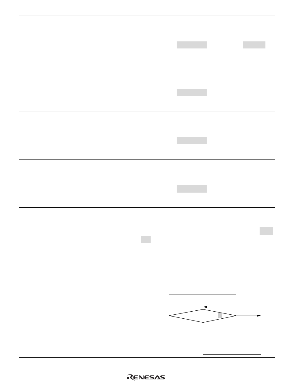
11.3.4 Non-Overlappng Pulse
Output
Figure 11-6 Setup Procedure for
Non-Overlapping Pulse Output
(Example)
510
Explanation amended as follows
[4] Set the SCI to the appropriate receive mode. Set
the RIE bit in SCR to 1 to enable the reception data
full (RXI) interrupt. Since the generation of receive
error during the SCI reception operation will disable
subsequent reception, the CPU should be enabled
to accept receive error interrupt.
Figure amended
TPU setup
Start counter
Compare match A?
[10]
No
Yes
Set next pulse
output data
[11]
www.DataSheet4U.com
11 Page | ||
| Páginas | Total 30 Páginas | |
| PDF Descargar | [ Datasheet HD6472394.PDF ] | |
Hoja de datos destacado
| Número de pieza | Descripción | Fabricantes |
| HD6472390 | (HD6472357 Series) 16-Bit Microcomputer | Renesas |
| HD6472392 | (HD6472357 Series) 16-Bit Microcomputer | Renesas |
| HD6472393 | (HD6472355 Series) Series of Microcomputers Built Around The H8s/2000 Cpu | Renesas |
| HD6472394 | (HD6472357 Series) 16-Bit Microcomputer | Renesas |
| Número de pieza | Descripción | Fabricantes |
| SLA6805M | High Voltage 3 phase Motor Driver IC. |
Sanken |
| SDC1742 | 12- and 14-Bit Hybrid Synchro / Resolver-to-Digital Converters. |
Analog Devices |
|
DataSheet.es es una pagina web que funciona como un repositorio de manuales o hoja de datos de muchos de los productos más populares, |
| DataSheet.es | 2020 | Privacy Policy | Contacto | Buscar |
