No Preview Available !

www.DataSheet4U.com
S29AL016D
16 Megabit (2 M x 8-Bit/1 M x 16-Bit)
CMOS 3.0 Volt-only Boot Sector Flash Memory
Data Sheet
PRELIMINARY
Distinctive Characteristics
Architectural Advantages
Ultra low power consumption (typical values
Single power supply operation
at 5 MHz)
— Full voltage range: 2.7 to 3.6 volt read and write op-
erations for battery-powered applications
— 200 nA Automatic Sleep mode current
— 200 nA standby mode current
Manufactured on 200nm process technology
— Fully compatible with 0.23 µm Am29LV160D and
MBM29LV160E devices
— 9 mA read current
— 20 mA program/erase current
Cycling endurance: 1,000,000 cycles per
Flexible sector architecture
— One 16 Kbyte, two 8 Kbyte, one 32 Kbyte, and thirty-
sector typical
Data retention: 20 years typical
one 64 Kbyte sectors (byte mode)
— One 8 Kword, two 4 Kword, one 16 Kword, and thirty-
one 32 Kword sectors (word mode)
Package Options
48-ball FBGA
Sector Protection features
— A hardware method of locking a sector to prevent any
48-pin TSOP
44-pin SOP
program or erase operations within that sector
— Sectors can be locked in-system or via programming
Software Features
equipment
DataSheet4U.cCoFmI (Common Flash Interface) compliant
— Temporary Sector Unprotect feature allows code
— Provides device-specific information to the system,
changes in previously locked sectors
allowing host software to easily reconfigure for
Unlock Bypass Program Command
different Flash devices
— Reduces overall programming time when issuing
Erase Suspend/Erase Resume
multiple program command sequences
— Suspends an erase operation to read data from, or
Top or bottom boot block configurations
available
Compatibility with JEDEC standards
— Pinout and software compatible with single-power
supply Flash
program data to, a sector that is not being erased,
then resumes the erase operation
Data# Polling and toggle bits
— Provides a software method of detecting program or
erase operation completion
— Superior inadvertent write protection
Hardware Features
Performance Characteristics
High performance
— Access times as fast as 70 ns
Ready/Busy# pin (RY/BY#)
— Provides a hardware method of detecting program or
erase cycle completion
DataShee
DataSheet4U.com
DataSheet4 U .com
Publication Number S29AL016D_00 Revision A Amendment 2 Issue Date December 17, 2004
DataSheet4U.com
1 page


www.DataSheet4U.com
Preliminary
Product Selector Guide
Family Part Number
Speed Option
Voltage Range: VCC = 2.7–3.6 V
Max access time, ns (tACC)
Max CE# access time, ns (tCE)
Max OE# access time, ns (tOE)
Note: See AC Characteristics for full specifications.
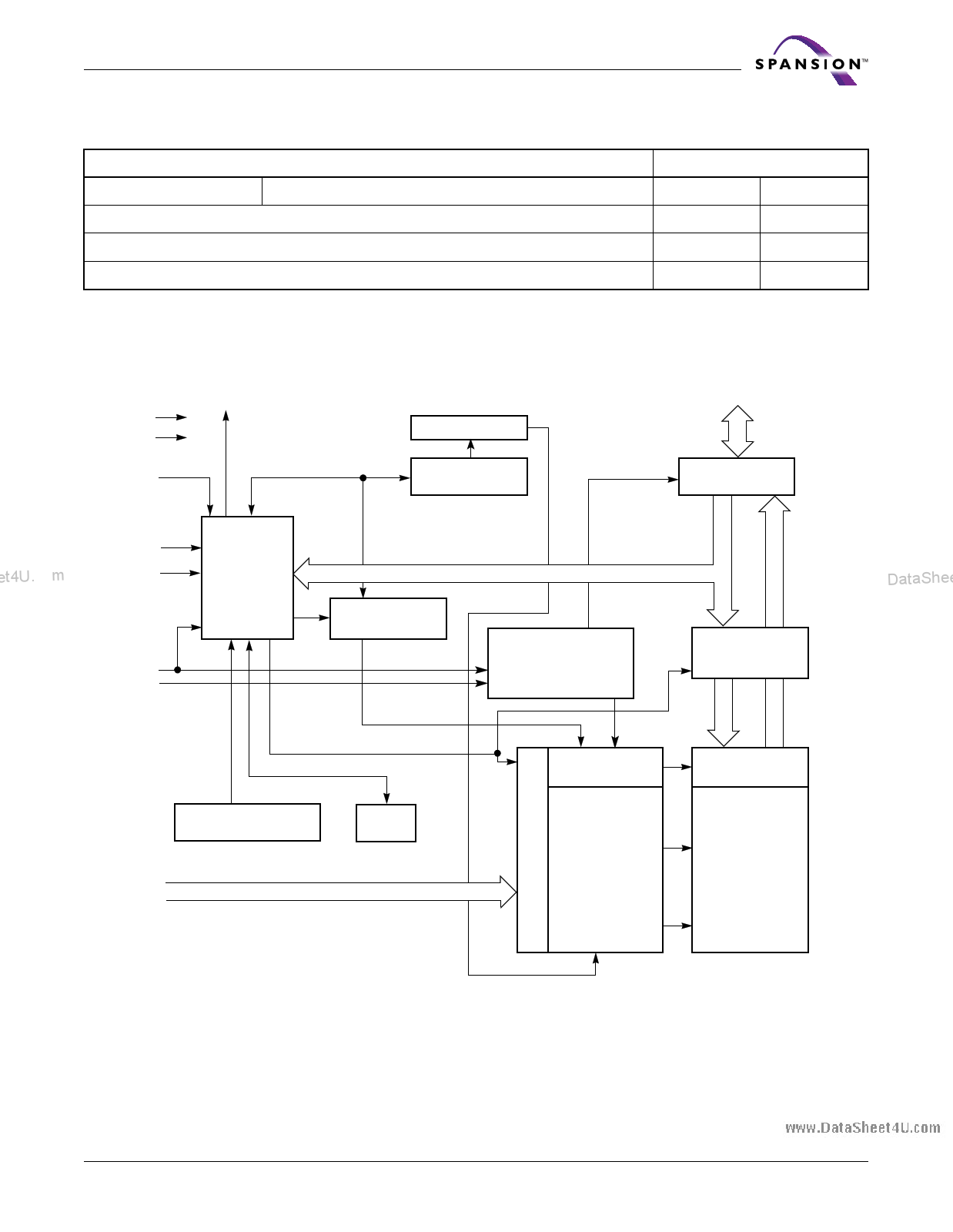
Block Diagram
VCC
VSS
RESET#
RY/BY#
Sector Switches
Erase Voltage
Generator
et4U.com
WE#
BYTE#
CE#
OE#
State
Control
Command
Register
PGGMenVeroalttaogrDeataSheet4U.com
Chip Enable
Output Enable
Logic
S29AL016D
70 90
70 90
70 90
30 35
DQ0–DQ15 (A-1)
Input/Output
Buffers
Data
STB Latch
DataShee
VCC Detector
A0–A19
Timer
Y-Decoder
STB
X-Decoder
Y-Gating
Cell Matrix
DataSheet4U.com
December 17, 2004 S29AL016D_00_A2
DataSheet4 U .com
S29AL016D
DataSheet4U.com
5
5 Page


www.DataSheet4U.com
Preliminary
Requirements for Reading Array Data
To read array data from the outputs, the system must drive the CE# and OE# pins
to VIL. CE# is the power control and selects the device. OE# is the output control
and gates array data to the output pins. WE# should remain at VIH. The BYTE#
pin determines whether the device outputs array data in words or bytes.
The internal state machine is set for reading array data upon device power-up,
or after a hardware reset. This ensures that no spurious alteration of the mem-
ory content occurs during the power transition. No command is necessary in
this mode to obtain array data. Standard microprocessor read cycles that as-
sert valid addresses on the device address inputs produce valid data on the
device data outputs. The device remains enabled for read access until the com-
mand register contents are altered.
See Reading Array Data for more information. Refer to the AC Read Operations
table for timing specifications and to Figure 13 for the timing diagram. ICC1 in the
DC Characteristics table represents the active current specification for reading ar-
ray data.
Writing Commands/Command Sequences
et4U.com
To write a command or command sequence (which includes programming data
to the device and erasing sectors of memory), the system must drive WE# and
CE# to VIL, and OE# to VIH.
For program operations, the BYTE# pin determines whether the device accepts
program data in bytes or words. See Word/Byte Configuration for more
information.
The device features an UnlockDBatyapSahsesemt4Uod.ceotmo facilitate faster programming.
Once the device enters the Unlock Bypass mode, only two write cycles are re-
quired to program a word or byte, instead of four. Word/Byte Program Command
Sequence has details on programming data to the device using both standard and
Unlock Bypass command sequences.
An erase operation can erase one sector, multiple sectors, or the entire device.
Tables 2 and 3 indicate the address space that each sector occupies. A “sector
address” consists of the address bits required to uniquely select a sector. The
Command Definitions section has details on erasing a sector or the entire chip,
or suspending/resuming the erase operation.
After the system writes the autoselect command sequence, the device enters the
autoselect mode. The system can then read autoselect codes from the internal
register (which is separate from the memory array) on DQ7–DQ0. Standard read
cycle timings apply in this mode. Refer to the Autoselect Mode and Autoselect
Command Sequence sections for more information.
ICC2 in the DC Characteristics table represents the active current specification for
the write mode. The AC Characteristics section contains timing specification ta-
bles and timing diagrams for write operations.
Program and Erase Operation Status
During an erase or program operation, the system may check the status of the
operation by reading the status bits on DQ7–DQ0. Standard read cycle timings
and ICC read specifications apply. Refer to Write Operation Status for more infor-
mation, and to AC Characteristics for timing diagrams.
DataSheet4U.com
December 17, 2004 S29AL016D_00_A2
DataSheet4 U .com
S29AL016D
DataSheet4U.com
DataShee
11
11 Page
| 


