|
|
|
PDF NCV7356 Data sheet ( Hoja de datos )
| Número de pieza | NCV7356 | |
| Descripción | Single Wire CAN Transceiver | |
| Fabricantes | ON Semiconductor | |
| Logotipo | ||
Hay una vista previa y un enlace de descarga de NCV7356 (archivo pdf) en la parte inferior de esta página. Total 24 Páginas | ||
|
No Preview Available !
NCV7356
Single Wire CAN Transceiver
The NCV7356 is a physical layer device for a single wire data link
capable of operating with various Carrier Sense Multiple Access
with Collision Resolution (CSMA/CR) protocols such as the Bosch
Controller Area Network (CAN) version 2.0. This serial data link
network is intended for use in applications where high data rate is not
required and a lower data rate can achieve cost reductions in both the
physical media components and in the microprocessor and/or
dedicated logic devices which use the network.
The network shall be able to operate in either the normal data rate
mode or a high−speed data download mode for assembly line and
service data transfer operations. The high−speed mode is only
intended to be operational when the bus is attached to an off−board
service node. This node shall provide temporary bus electrical loads
which facilitate higher speed operation. Such temporary loads should
be removed when not performing download operations.
The bit rate for normal communications is typically 33 kbit/s, for
high−speed transmissions like described above a typical bit rate of
83 kbit/s is recommended. The NCV7356 features undervoltage
lockout, timeout for faulty blocked input signals, output blanking
time in case of bus ringing and a very low sleep mode current.
The device is compliant with GMW3089V2.4
General Motors Corporation specification.
Features
• Fully Compatible with J2411 Single Wire CAN Specification
• 60 mA (max) Sleep Mode Current
• Operating Voltage Range 5.0 to 27 V
• Up to 100 kbps High−Speed Transmission Mode
• Up to 40 kbps Bus Speed
• Selective BUS Wake−Up
• Logic Inputs Compatible with 3.3 V and 5 V Supply Systems
• Control Pin for External Voltage Regulators (14 Pin Package Only)
• Standby to Sleep Mode Timeout
• Low RFI Due to Output Wave Shaping
• Fully Integrated Receiver Filter
• Bus Terminals Short−Circuit and Transient Proof
• Loss of Ground Protection
• Protection Against Load Dump, Jump Start
• Thermal Overload and Short Circuit Protection
• ESD Protection of 4.0 kV on CANH Pin (2.0 kV on Any Other Pin)
• Undervoltage Lock Out
• Bus Dominant Timeout Feature
• Internally Fused Leads in SO−14 Package
• NCV Prefix for Automotive and Other Applications Requiring
Unique Site and Control Change Requirements; AEC−Q100
Qualified and PPAP Capable
• These Devices are Pb−Free and are RoHS Compliant
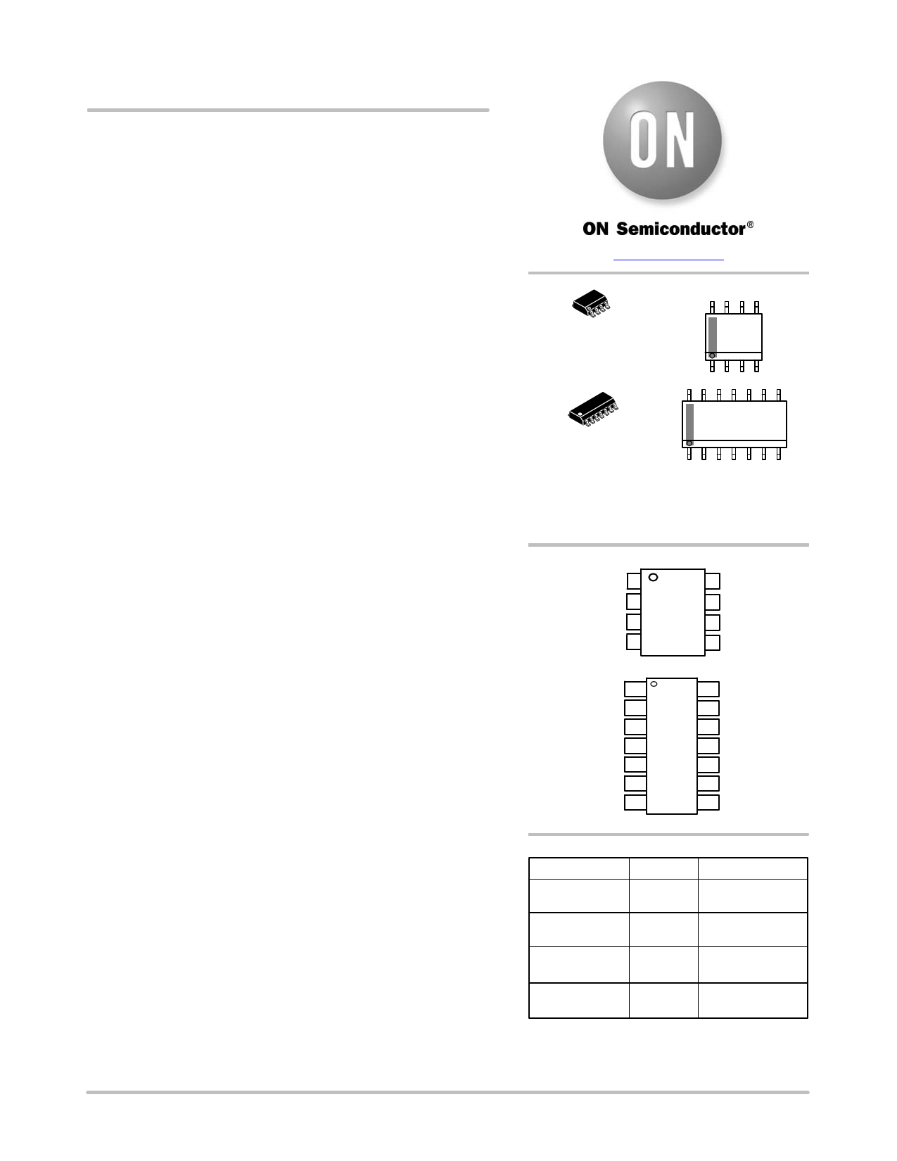
www.onsemi.com
8
1
SOIC−8
D SUFFIX
CASE 751
14
1
SOIC−14
D SUFFIX
CASE 751A
MARKING DIAGRAMS
8
V7356
ALYW
G
1
14
NCV7356G
AWLYWW
1
A = Assembly Location
WL, L = Wafer Lot
Y = Year
WW, W = Work Week
G or G = Pb−Free Package
PIN CONNECTIONS
TxD 1
8 GND
MODE0 2
7 CANH
MODE1 3
6 LOAD
RxD 4
5 VBAT
(Top View)
GND 1
TxD 2
MODE0 3
MODE1 4
RxD 5
NC 6
GND 7
14 GND
13 NC
12 CANH
11 LOAD
10 VBAT
9 INH
8 GND
(Top View)
ORDERING INFORMATION
Device
Package
Shipping†
NCV7356D1G
SOIC−8
(Pb−Free)
98 Units / Rail
NCV7356D1R2G SOIC−8 2500 Tape & Reel
(Pb−Free)
NCV7356D2G
SOIC−14
(Pb−Free)
55 Units / Rail
NCV7356D2R2G SOIC−14 2500 Tape & Reel
(Pb−Free)
†For information on tape and reel specifications,
including part orientation and tape sizes, please
refer to our Tape and Reel Packaging Specification
Brochure, BRD8011/D.
© Semiconductor Components Industries, LLC, 2016
September, 2016 − Rev. 12
1
Publication Order Number:
NCV7356/D
1 page 
NCV7356
Electrical Specification
All voltages are referenced to ground (GND). Positive
currents flow into the IC. The maximum ratings given in
the table below are limiting values that do not lead to a
permanent damage of the device but exceeding any of these
limits may do so. Long term exposure to limiting values
may affect the reliability of the device.
MAXIMUM RATINGS
Rating
Symbol
Condition
Min Max Unit
Supply Voltage, Normal Operation
Short−Term Supply Voltage, Transient
VBAT
VBAT.LD
−
Load Dump; t < 500 ms
Jump Start; t < 1.0 min
−0.3 18
V
− 40 V (peak)
− 27 V
Transient Supply Voltage
Transient Supply Voltage
Transient Supply Voltage
CANH Voltage
VBAT.TR1
VBAT.TR2
VBAT.TR3
VCANH
Transient Bus Voltage
Transient Bus Voltage
Transient Bus Voltage
DC Voltage on Pin LOAD
DC Voltage on Pins TxD, MODE1, MODE0, RxD
ESD Capability of CANH
(Note 4)
VCANHTR1
VCANHTR2
VCANHTR3
VLOAD
VDC
VESDBUS
ISO 7637/1 Pulse 1 (Note 2)
ISO 7637/1 Pulses 2 (Note 2)
ISO 7637/1 Pulses 3A, 3B
VBAT < 27 V
VBAT = 0 V
ISO 7637/1 Pulse 1 (Note 3)
ISO 7637/1 Pulses 2 (Note 3)
ISO 7637/1 Pulses 3A, 3B (Note 3)
Via RT > 2.0 kW
−
Human Body Model
(with respect to VBAT and GND)
Eq. to Discharge 100 pF with 1.5 kW
−50
−
−200
−20
−40
−50
−
−200
−40
−0.3
−4000
−
100
200
40
−
100
200
40
7.0
4000
V
V
V
V
V
V
V
V
V
V
ESD Capability of Any Other Pin
(Note 4)
VESD
Human Body Model
Eq. to Discharge 100 pF with 1.5 kW
−2000
2000
V
Maximum Latchup Free Current at Any Pin
ILATCH
−
Storage Temperature
TSTG
−
Junction Temperature
TJ −
Peak Reflow Soldering Temperature: Pb−Free, 60 s to 150 s above 217°C (Note 5)
−500
−55
−40
500
150
150
260
mA
°C
°C
°C
Stresses exceeding those listed in the Maximum Ratings table may damage the device. If any of these limits are exceeded, device functionality
should not be assumed, damage may occur and reliability may be affected.
2. ISO 7637 test pulses are applied to VBAT via a reverse polarity diode and >1.0 mF blocking capacitor.
3. ISO 7637 test pulses are applied to CANH via a coupling capacitance of 1.0 nF.
4. ESD measured per Q100−002 (EIA/JESD22−A114−A).
5. For additional information, please see or download the ON Semiconductor Soldering and Mounting Techniques Reference Manual,
SOLDERRM/D.
TYPICAL THERMAL CHARACTERISTICS
Test Condition, Typical Value
Parameter
Min Pad Board
1, Pad Board
Unit
SOIC−8
Junction−to−Lead (psi−JL7, YJL8) or Pins 6−7
Junction−to−Ambient (RqJA, qJA)
SOIC−14
57 (Note 6)
187 (Note 6)
51 (Note 7)
128 (Note 7)
°C/W
°C/W
Junction−to−Lead (psi−JL8, YJL8)
Junction−to−Ambient (RqJA, qJA)
6. 1 oz copper, 53 mm2 coper area, 0.062″ thick FR4.
7. 1 oz copper, 716 mm2 coper area, 0.062″ thick FR4.
8. 1 oz copper, 94 mm2 coper area, 0.062″ thick FR4.
9. 1 oz copper, 767 mm2 coper area, 0.062″ thick FR4.
30 (Note 8)
122 (Note 8)
30 (Note 9)
84 (Note 9)
°C/W
°C/W
www.onsemi.com
5
5 Page 
NCV7356
FUNCTIONAL DESCRIPTION
TxD Input Pin
TxD Polarity
• TxD = logic 1 (or floating) on this pin produces an
undriven or recessive bus state (low bus voltage)
• TxD = logic 0 on this pin produces either a bus normal
or a bus high voltage dominant state depending on the
transceiver mode state (high bus voltage)
If the TxD pin is driven to a logic low state while the sleep
mode (Mode 0 = 0 and Mode 1 = 0) is activated, the
transceiver can not drive the CANH pin to the dominant
state.
The transceiver provides an internal pullup current on the
TxD pin which will cause the transmitter to default to the
bus recessive state when TxD is not driven.
TxD input signals are standard CMOS logic levels.
Timeout Feature
In case of a faulty blocked dominant TxD input signal,
the CANH output is switched off automatically after the
specified TxD timeout reaction time to prevent a dominant
bus.
The transmission is continued by next TxD L to H
transition without delay.
MODE0 and MODE1 Pins
The transceiver provides a weak internal pulldown
current on each of these pins which causes the transceiver
to default to sleep mode when they are not driven. The
mode input signals are standard CMOS logic level for
3.3 V and 5 V supply voltages. See Electrical
Characteristics table for timing limitations for mode
changes.
MODE0
L
H
L
H
MODE1
L
L
H
H
Mode
Sleep Mode
High−Speed Mode
High Voltage Wake−Up
Normal Mode
Sleep Mode
Transceiver is in low power state, waiting for wake−up
via high voltage signal or by mode pins change to any state
other than 0,0. In this state, the CANH pin is not in the
dominant state regardless of the state of the TxD pin.
High−Speed Mode
This mode allows high−speed download with bit rates up
to 100 Kbit/s. The output wave shapingaping circuit is
disabled in this mode. Bus transmitter drive circuits for
those nodes which are required to communicate in
high−speed mode are able to drive reduced bus resistance
in this mode.
High Voltage Wake−Up Mode
This bus includes a selective node awake capability,
which allows normal communication to take place among
some nodes while leaving the other nodes in an undisturbed
sleep state. This is accomplished by controlling the signal
voltages such that all nodes must wake−up when they
receive a higher voltage message signal waveform. The
communication system communicates to the nodes
information as to which nodes are to stay operational
(awake) and which nodes are to put themselves into a non
communicating low power “sleep” state. Communication
at the lower, normal voltage levels shall not disturb the
sleeping nodes.
Normal Mode
Transmission bit rate in normal communication is
33 Kbits/s. In normal transmission mode the NCV7356
supports controlled waveform rise and overshoot times.
Waveform trailing edge control is required to assure that
high frequency components are minimized at the
beginning of the downward voltage slope. The remaining
fall time occurs after the bus is inactive with drivers off and
is determined by the RC time constant of the total bus load.
RxD Output Pin
Logic data as sensed on the single wire CAN bus.
RxD Polarity
• RxD = logic 1 on this pin indicates a bus recessive
state (low bus voltage)
• RxD = logic 0 on this pin indicates a bus normal or
high voltage bus dominant state
RxD in Sleep Mode
RxD does not pass signals to the microprocessor while in
sleep mode until a valid wake−up bus voltage level is
received or the MODE0 and MODE 1 pins are not 0, 0
respectively. When the valid wake−up bus voltage signal
awakens the transceiver, the RxD pin signals an interrupt
(logic 0). If there is no mode change within 250 ms (typ),
the transceiver re−enters the sleep mode.
When not in sleep mode all valid bus signals will be sent
out on the RxD pin.
RxD will be placed in the undriven or off state when in
sleep mode.
RxD Typical Load
Resistance: 2.7 kW
Capacitance: < 25 pF
www.onsemi.com
11
11 Page | ||
| Páginas | Total 24 Páginas | |
| PDF Descargar | [ Datasheet NCV7356.PDF ] | |
Hoja de datos destacado
| Número de pieza | Descripción | Fabricantes |
| NCV7351 | High Speed CAN Transceiver | ON Semiconductor |
| NCV7351F | High Speed CAN Transceiver | ON Semiconductor |
| NCV7356 | Single Wire CAN Transceiver | ON Semiconductor |
| Número de pieza | Descripción | Fabricantes |
| SLA6805M | High Voltage 3 phase Motor Driver IC. |
Sanken |
| SDC1742 | 12- and 14-Bit Hybrid Synchro / Resolver-to-Digital Converters. |
Analog Devices |
|
DataSheet.es es una pagina web que funciona como un repositorio de manuales o hoja de datos de muchos de los productos más populares, |
| DataSheet.es | 2020 | Privacy Policy | Contacto | Buscar |