|
|
|
PDF HMN12816D Data sheet ( Hoja de datos )
| Número de pieza | HMN12816D | |
| Descripción | Non-Volatile SRAM MODULE 2Mbit | |
| Fabricantes | Hanbit | |
| Logotipo | ||
Hay una vista previa y un enlace de descarga de HMN12816D (archivo pdf) en la parte inferior de esta página. Total 9 Páginas | ||
|
No Preview Available !
www.DataSheet4U.com
HANBit
HMN12816D
Non-Volatile SRAM MODULE 2Mbit (128K x 16-Bit), 40pin-Dip, 5V
Part No. HMN12816D
GENERAL DESCRIPTION
The HMN12816D 128K x 16 nonvolatile SRAM’s are 2,097,152-bit fully static, nonvolatile SRAM’s, organized as
131,072 words by 16 bits. Each NVSRAM has a self contained lithium energy source and control circuitry which
constantly monitors Vcc for an out-of-tolerance condition. When such a condition occurs, the lithium energy source is
automatically switched on and write protection is unconditionally enabled to prevent data corruption. DIP-package
HMN12816D devices can be used in place of solutions which build nonvolatile 128Kx16 memory by utilizing a
variety of discrete components. There is no limit on the number of write cycles that can be executed and no additional
support circuitry is required for microprocessor interfacing.
The HMN12816D uses extremely low standby current CMOS SRAM’s, coupled with small lithium coin cells to provide non-
volatility without long write-cycle times and the write-cycle limitations associated with EEPROM.
FEATURES
w Access time : 70, 85, 120, 150ns
w High-density design : 256KByte Design
w Battery internally isolated until power is applied
w Industry-standard 40-pin 128K x 16 pinout
w Unlimited write cycles
w Data retention in the absence of VCC
w 10-years minimum data retention in absence of power
w Automatic write-protection during power-up/power-down
cycles
w Data is automatically protected during power loss
w Conventional SRAM operation; unlimited write cycles
OPTIONS
w Timing
70 ns
85 ns
120 ns
150 ns
MARKING
- 70
- 85
-120
-150
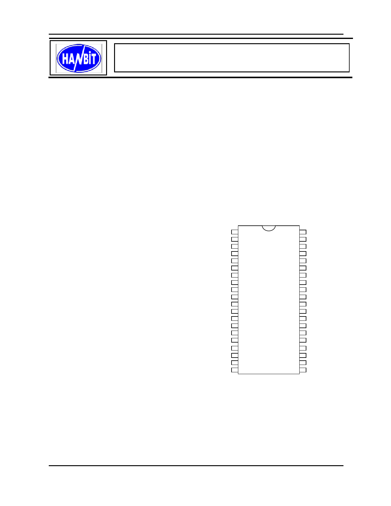
PIN ASSIGNMENT
/CEU
/CEL
DQ15
DQ14
DQ13
DQ12
DQ11
DQ10
DQ9
DQ8
Vss
DQ7
DQ6
DQ5
DQ4
DQ3
DQ2
DQ1
DQ0
/OE
1
2
3
4
5
6
7
8
9
10
11
12
13
14
15
16
17
18
19
20
40 Vcc
39 /WE
38 A16
37 A15
36 A14
35 A13
34 A12
33 A11
32 A10
31 A9
30 Vss
29 A8
28 A7
27 A6
26 A5
25 A4
24 A3
23 A2
22 A1
21 A0
40-pin Encapsulated Package
URL : www.hbe.co.kr
Rev. 0.0 (April, 2002)
1 HANBit Electronics Co.,Ltd
1 page 
HANBit
HMN12816D
READ CYCLE (TA= TOPR, VCCmin £ VCC≤ VCCmax )
PARAMETER
SYMBOL CONDITIONS
-70
MIN MAX
Read Cycle Time
tRC
70 -
Address Access Time
tACC Output load A - 70
Chip enable access time
tACE Output load A - 70
Output enable to Output valid
tOE Output load A - 35
Chip enable to output in low Z
tCLZ
Output load B
5
-
Output enable to output in low Z
tOLZ
Output load B
5
-
Chip disable to output in high Z
tCHZ Output load B 0 25
Output disable to output high Z
tOHZ Output load B 0 25
Output hold from address change
tOH
Output load A 10
-
-85
MIN MAX
85 -
- 85
- 85
- 45
5-
0-
0 35
0 25
10 -
-120
MIN MAX
120 -
- 120
- 120
- 60
5-
0-
0 45
0 35
10 -
-150
MIN MAX
150 -
- 150
- 150
- 70
10 -
5-
0 60
0 50
10 -
UNIT
ns
ns
ns
ns
ns
ns
ns
ns
ns
WRITE CYCLE (TA= TOPR, Vccmin £ Vcc ≤ Vccmax )
PARAMETER
SYMBOL CONDITIONS
-70
MIN MAX
-85
MIN MAX
-120
MIN MAX
-150
Min Max
Write Cycle Time
tWC
70 - 85 - 120 - 150 -
Chip enable to end of write
tCW
Note 1
65 - 75 - 100 - 100 -
Address setup time
tAS
Note 2
0-0-0-0-
Address valid to end of write
tAW
Note 1
65 - 75 - 100 - 90 -
Write pulse width
tWP
Note 1
55 - 65 - 85 - 90 -
Write recovery time (write cycle 1)
tWR1
Note 3
5-5-5-5-
Write recovery time (write cycle 2)
tWR2
Note 3
15 - 15 - 15 - 15 -
Data valid to end of write
tDW
30 - 35 - 45 - 50 -
Data hold time (write cycle 1)
tDH1
Note 4
0-0-0-0-
Data hold time (write cycle 2)
tDH2
Note 4
10 - 10 - 10 - 0 -
Write enabled to output in high Z
tWZ
Note 5
0 25 0 30 0 40 0 50
Output active from end of write
tOW
Note 5
5-0-0-5-
NOTE: 1. A write ends at the earlier transition of /CE going high and /WE going high.
2. A write occurs during the overlap of allow /CE and a low /WE. A write begins at the later transition of /CE
going low and /WE going low.
3. Either tWR1 or tWR2 must be met.
4. Either tDH1 or tDH2 must be met.
5. If /CE goes low simultaneously with /WE going low or after /WE going low, the outputs remain in high-
impedance state.
UNI
T
ns
ns
ns
ns
ns
ns
ns
ns
ns
ns
ns
ns
URL : www.hbe.co.kr
Rev. 0.0 (April, 2002)
5 HANBit Electronics Co.,Ltd
5 Page | ||
| Páginas | Total 9 Páginas | |
| PDF Descargar | [ Datasheet HMN12816D.PDF ] | |
Hoja de datos destacado
| Número de pieza | Descripción | Fabricantes |
| HMN12816D | Non-Volatile SRAM MODULE 2Mbit | Hanbit |
| Número de pieza | Descripción | Fabricantes |
| SLA6805M | High Voltage 3 phase Motor Driver IC. |
Sanken |
| SDC1742 | 12- and 14-Bit Hybrid Synchro / Resolver-to-Digital Converters. |
Analog Devices |
|
DataSheet.es es una pagina web que funciona como un repositorio de manuales o hoja de datos de muchos de los productos más populares, |
| DataSheet.es | 2020 | Privacy Policy | Contacto | Buscar |