|
|
|
PDF HA7-5221-5 Data sheet ( Hoja de datos )
| Número de pieza | HA7-5221-5 | |
| Descripción | 100MHz/ Low Noise/ Precision Operational Amplifier | |
| Fabricantes | Intersil Corporation | |
| Logotipo | ||
Hay una vista previa y un enlace de descarga de HA7-5221-5 (archivo pdf) en la parte inferior de esta página. Total 12 Páginas | ||
|
No Preview Available !
TM
Data Sheet
HA-5221
April 2000 File Number 2915.5
100MHz, Low Noise, Precision
Operational Amplifier
The HA-5221 is a single high performance dielectrically
isolated, op amp, featuring precision DC characteristics while
providing excellent AC characteristics. Designed for audio,
video, and other demanding applications, noise (3.4nV/√Hz at
1kHz), total harmonic distortion (<0.005%), and DC errors are
kept to a minimum.
The precision performance is shown by low offset voltage
(0.3mV), low bias currents (40nA), low offset currents
(15nA), and high open loop gain (128dB). The combination
of these excellent DC characteristics with the fast settling
time (0.4µs) makes the HA-5221 ideally suited for precision
signal conditioning.
The unique design of the HA-5221 gives it outstanding AC
characteristics not normally associated with precision op
amps, high unity gain bandwidth (35MHz) and high slew rate
(25V/µs). Other key specifications include high CMRR (95dB)
and high PSRR (100dB). The combination of these
specifications will allow the HA-5221 to be used in RF signal
conditioning as well as video amplifiers.
For MIL-STD-883C compliant product and Ceramic LCC
packaging, consult the HA-5221/883C data sheet. (Intersil
AnswerFAX (321-724-7800) Document #3716.)
Ordering Information
PART NUMBER
(BRAND)
HA7-5221-5
HA9P5221-5
(H52215)
TEMP.
RANGE (oC)
PACKAGE
0 to 75 8 Ld CERDIP
0 to 75 8 Ld SOIC
PKG.
NO.
F8.3A
M8.15
Features
• Gain Bandwidth Product. . . . . . . . . . . . . . . . . . . . 100MHz
• Unity Gain Bandwidth. . . . . . . . . . . . . . . . . . . . . . . 35MHz
• Slew Rate . . . . . . . . . . . . . . . . . . . . . . . . . . . . . . . . 25V/µs
• Low Offset Voltage . . . . . . . . . . . . . . . . . . . . . . . . . 0.3mV
• High Open Loop Gain. . . . . . . . . . . . . . . . . . . . . . . 128dB
• Low Noise Voltage at 1kHz. . . . . . . . . . . . . . . . 3.4nV/√Hz
• High Output Current . . . . . . . . . . . . . . . . . . . . . . . . . 56mA
• Low Supply Current . . . . . . . . . . . . . . . . . . . . . . . . . . 8mA
Applications
• Precision Test Systems
• Active Filtering
• Small Signal Video
• Accurate Signal Processing
• RF Signal Conditioning
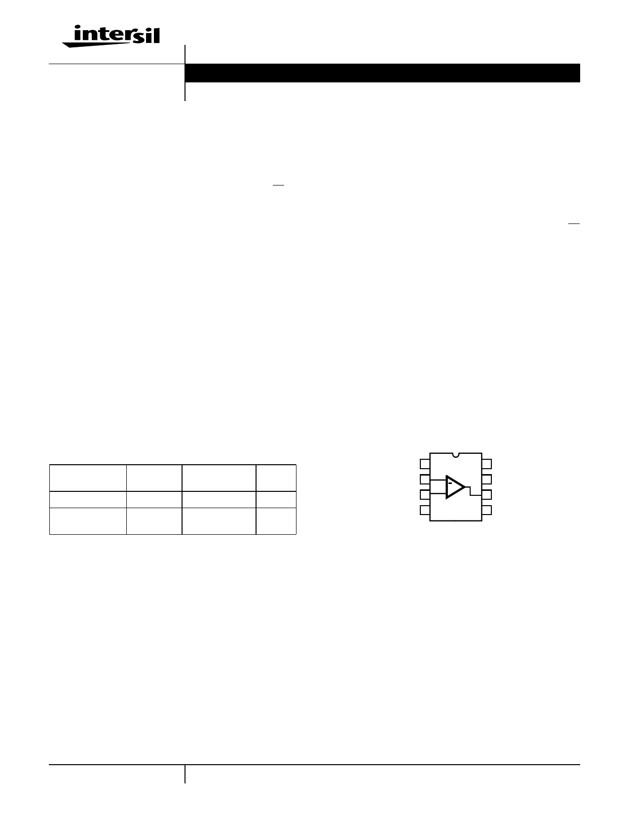
Pinout
HA-5221
(CERDIP, SOIC)
TOP VIEW
-BAL 1
-IN 2
+IN 3
V- 4
+
8 +BAL
7 V+
6 OUT
5 NC
1
CAUTION: These devices are sensitive to electrostatic discharge; follow proper IC Handling Procedures.
1-888-INTERSIL or 321-724-7143 | Intersil and Design is a trademark of Intersil Corporation. | Copyright © Intersil Corporation 2000
1 page 
HA-5221
Saturation Recovery
When an op amp is over driven, output devices can saturate
and sometimes take a long time to recover. By clamping the
input, output saturation can be avoided. If output saturation
can not be avoided, the maximum recovery time when
overdriven into the positive rail is 10.6µs. When driven into
the negative rail the maximum recovery time is 3.8µs.
Input Protection
The HA-5221 has built in back-to-back protection diodes
which limit the maximum allowable differential input voltage
to approximately 5V. If the HA-5221 is used in circuits where
the maximum differential voltage may be exceeded, then
current limiting resistors must be used. The input current
should be limited to a maximum of 10mA.
Typical Performance Curves VS = ±15V, TA = 25oC
RLIMIT2
∆VIN
RLIMIT3
6
+ VOUT
PC Board Layout Guidelines
When designing with the HA-5221, good high frequency
(RF) techniques should be used when building a PC board.
Use of ground plane is recommended. Power supply
decoupling is very important. A 0.01µF to 0.1µF high quality
ceramic capacitor at each power supply pin with a 2.2µF to
10µF tantalum close by will provide excellent decoupling.
Chip capacitors produce the best results due to ease of
placement next to the op amp and basically no lead
inductance. If leaded capacitors are used, the leads should
be kept as short as possible to minimize lead inductance.
RL = 1K, CL = 50pF
120
100
80 GAIN
60
40
20
0
PHASE
180
135
90
45
0
1K
10K 100K
1M
10M
100M
FREQUENCY (Hz)
FIGURE 5. OPEN LOOP GAIN AND PHASE vs FREQUENCY
12
9 AV = +1, RL = 1K, CL = 50pF
6
3 GAIN
0
-3
-6
PHASE
10K 100K 1M
10M
FREQUENCY (Hz)
180
135
90
45
0
100M
FIGURE 6. CLOSED LOOP GAIN vs FREQUENCY
9
6 AV = -1, RL = 1K, CL = 50pF
3
GAIN
0
PHASE
180
135
90
45
0
10K 100K
1M
10M
100M
FREQUENCY (Hz)
FIGURE 7. CLOSED LOOP GAIN vs FREQUENCY
80
60 AV = -1000
40 AV = -100
20 AV = -10
0
AV = -10
AV = -1000
RL = 1K, CL = 50pF
AV = -100
180
135
90
45
0
10K 100K
1M
10M
100M
FREQUENCY (Hz)
FIGURE 8. VARIOUS CLOSED LOOP GAINS vs FREQUENCY
5
5 Page 
HA-5221
Ceramic Dual-In-Line Frit Seal Packages (CERDIP)
c1 LEAD FINISH
-A- -D-
E
-B-
bbb S C A - B S D S
BASE
METAL
(c)
b1
MM
(b)
SECTION A-A
BASE
PLANE
SEATING
PLANE
S1
b2
b
D
AA
e
Q
-C- A
L
eA/2
α
eA
c
ccc M C A - B S D S
aaa M C A - B S D S
NOTES:
1. Index area: A notch or a pin one identification mark shall be locat-
ed adjacent to pin one and shall be located within the shaded
area shown. The manufacturer’s identification shall not be used
as a pin one identification mark.
2. The maximum limits of lead dimensions b and c or M shall be
measured at the centroid of the finished lead surfaces, when
solder dip or tin plate lead finish is applied.
3. Dimensions b1 and c1 apply to lead base metal only. Dimension
M applies to lead plating and finish thickness.
4. Corner leads (1, N, N/2, and N/2+1) may be configured with a
partial lead paddle. For this configuration dimension b3 replaces
dimension b2.
5. This dimension allows for off-center lid, meniscus, and glass
overrun.
6. Dimension Q shall be measured from the seating plane to the
base plane.
7. Measure dimension S1 at all four corners.
8. N is the maximum number of terminal positions.
9. Dimensioning and tolerancing per ANSI Y14.5M - 1982.
10. Controlling dimension: INCH
F8.3A MIL-STD-1835 GDIP1-T8 (D-4, CONFIGURATION A)
8 LEAD CERAMIC DUAL-IN-LINE FRIT SEAL PACKAGE
INCHES
MILLIMETERS
SYMBOL MIN MAX MIN MAX NOTES
A - 0.200 - 5.08 -
b
0.014
0.026
0.36
0.66
2
b1
0.014
0.023
0.36
0.58
3
b2
0.045
0.065
1.14
1.65
-
b3
0.023
0.045
0.58
1.14
4
c
0.008
0.018
0.20
0.46
2
c1
0.008
0.015
0.20
0.38
3
D - 0.405 - 10.29 5
E
0.220
0.310
5.59
7.87
5
e 0.100 BSC
2.54 BSC
-
eA 0.300 BSC
7.62 BSC
-
eA/2
0.150 BSC
3.81 BSC
-
L
0.125
0.200
3.18
5.08
-
Q
0.015
0.060
0.38
1.52
6
S1 0.005 - 0.13 - 7
α
90o 105o 90o 105o
-
aaa - 0.015 - 0.38 -
bbb - 0.030 - 0.76 -
ccc - 0.010 - 0.25 -
M
-
0.0015
-
0.038
2, 3
N8
88
Rev. 0 4/94
11
11 Page | ||
| Páginas | Total 12 Páginas | |
| PDF Descargar | [ Datasheet HA7-5221-5.PDF ] | |
Hoja de datos destacado
| Número de pieza | Descripción | Fabricantes |
| HA7-5221-5 | 100MHz/ Low Noise/ Precision Operational Amplifier | Intersil Corporation |
| Número de pieza | Descripción | Fabricantes |
| SLA6805M | High Voltage 3 phase Motor Driver IC. |
Sanken |
| SDC1742 | 12- and 14-Bit Hybrid Synchro / Resolver-to-Digital Converters. |
Analog Devices |
|
DataSheet.es es una pagina web que funciona como un repositorio de manuales o hoja de datos de muchos de los productos más populares, |
| DataSheet.es | 2020 | Privacy Policy | Contacto | Buscar |