|
|
|
PDF ZL50061 Data sheet ( Hoja de datos )
| Número de pieza | ZL50061 | |
| Descripción | (ZL50060 / ZL50061) 16 K-Channel Digital Switch | |
| Fabricantes | Zarlink Semiconductor | |
| Logotipo | ||
Hay una vista previa y un enlace de descarga de ZL50061 (archivo pdf) en la parte inferior de esta página. Total 30 Páginas | ||
|
No Preview Available !
www.DataSheet4U.com
ZL50060/1
16 K-Channel Digital Switch with High Jitter
Tolerance, Per Stream Rate Conversion (2, 4, 8,
16, or 32 Mbps), and 64 Inputs and 64 Outputs
Data Sheet
Features
• 16,384-channel x 16,384-channel non-blocking
unidirectional switching.The Backplane and Local
inputs and outputs can be combined to form a
non-blocking switching matrix with 64 input
streams and 64 output streams
• 8,192-channel x 8,192-channel non-blocking
Backplane input to Local output stream switch
• 8,192-channel x 8,192-channel non-blocking
Local input to Backplane output stream switch
• 8,192-channel x 8,192-channel non-blocking
Backplane input to Backplane output switch
• 8,192-channel x 8,192-channel non-blocking
Local input to Local output stream switch
• Rate conversion on all data paths, Backplane-to-
Local, Local-to-Backplane, Backplane-to-
Backplane and Local-to-Local streams
• Backplane port accepts 32 input and 32 output
ST-BUS streams with data rates of 2.048 Mbps,
4.096 Mbps, 8.192 Mbps or 16.384 Mbps in any
combination, or a fixed allocation of 16 input and
16 output streams at 32.768 Mbps
• Local port accepts 32 input and 32 output ST-
BUS streams with data rates of 2.048 Mbps,
February 2006
Ordering Information
ZL50060GAC
ZL50060GAG2
ZL50061GAG
ZL50061GAG2
256 Ball PBGA
256 Ball PBGA**
272 Ball PBGA
272 Ball PBGA**
**Pb Free Tin/Silver/Copper
-40°C to +85°C
Trays
Trays
Trays
Trays
4.096 Mbps, 8.192 Mbps or 16.384 Mbps in any
combination, or a fixed allocation of 16 input and
16 output streams at 32.768 Mbps
• Exceptional input clock jitter tolerance (17 ns for
16 Mbps or lower data rates, 14 ns for 32 Mbps)
• Per-stream channel and bit delay for Local and
Backplane input streams
• Per-stream advancement for Local and Backplane
output streams
• Constant 2-frame throughput delay for frame
integrity
• Per-channel high impedance output control for
Local and Backplane streams
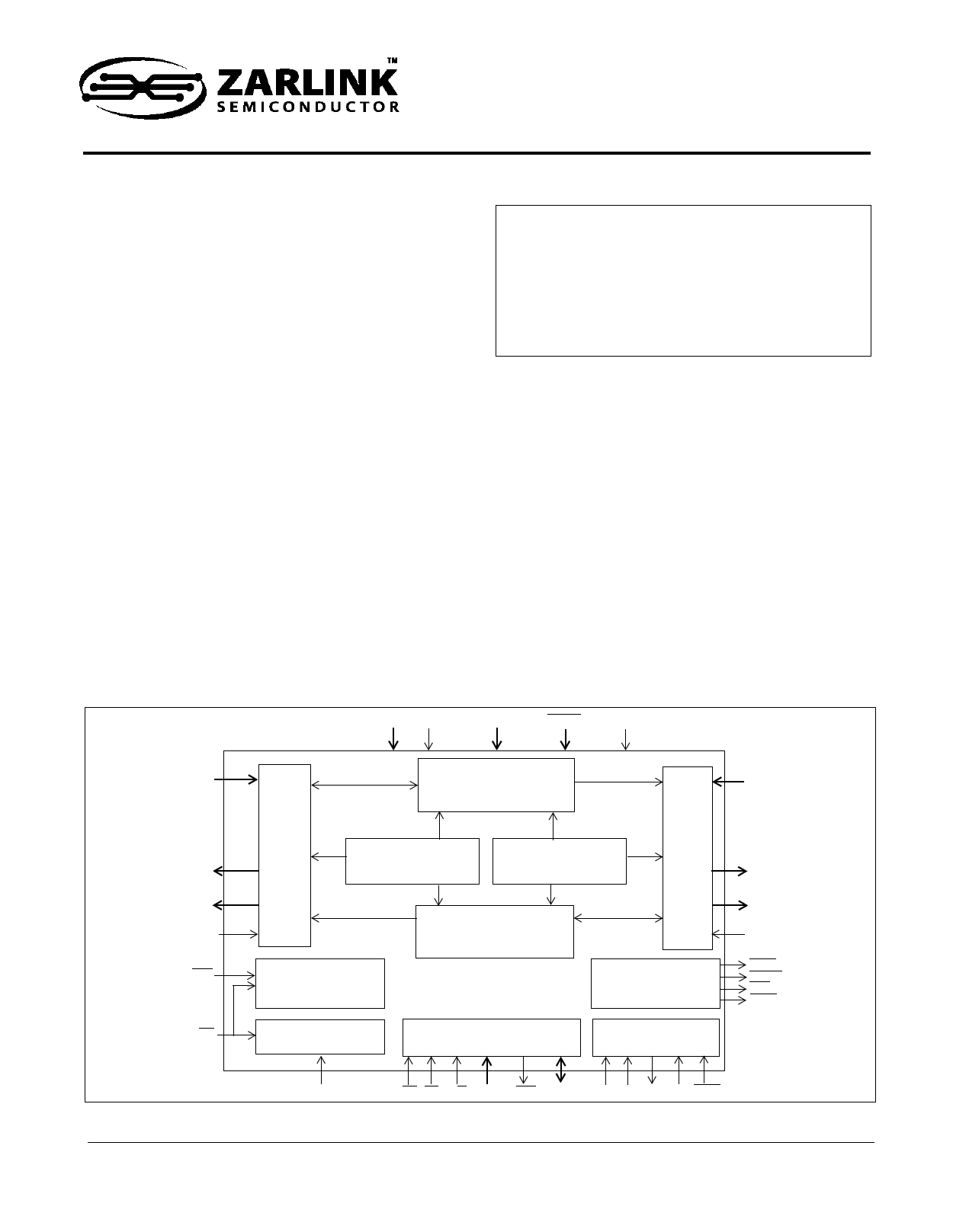
VDD_IO VDD_CORE
VSS (GND)
RESET
ODE
BSTi0-31
Backplane Data Memories
(8,192 channels)
Local
Interface
LSTi0-31
BSTo0-31
BCST0-3
BORS
FP8i
C8i
Backplane
Interface
Backplane
Connection Memory
(8,192 locations)
Local
Connection Memory
(8,192 locations)
Local
Interface
Input
Timing Unit
PLL
Local Data Memories
(8,192 channels)
Microprocessor Interface
and Internal Registers
Output
Timing
Unit
Test Port
LSTo0-31
LCST0-3
LORS
FP8o
FP16o
C8o
C16o
VDD_PLL
DS CS R/W A14-0 DTA D15-0 TMS TDi TDo TCK TRST
Figure 1 - ZL50060/1 Functional Block Diagram
1
Zarlink Semiconductor Inc.
Zarlink, ZL and the Zarlink Semiconductor logo are trademarks of Zarlink Semiconductor Inc.
Copyright 2003-2006, Zarlink Semiconductor Inc. All Rights Reserved.
1 page 
ZL50060/1
Data Sheet
Table of Contents
11.2.2.3 The Device Identification Register . . . . . . . . . . . . . . . . . . . . . . . . . . . . . . . . . . . . . . . . . . . . 50
11.3 Boundary Scan Description Language (BSDL) File . . . . . . . . . . . . . . . . . . . . . . . . . . . . . . . . . . . . . . . . 50
12.0 Memory Address Mappings . . . . . . . . . . . . . . . . . . . . . . . . . . . . . . . . . . . . . . . . . . . . . . . . . . . . . . . . . . . . 51
12.1 Local Data Memory Bit Definition . . . . . . . . . . . . . . . . . . . . . . . . . . . . . . . . . . . . . . . . . . . . . . . . . . . . . . 51
12.2 Backplane Data Memory Bit Definition . . . . . . . . . . . . . . . . . . . . . . . . . . . . . . . . . . . . . . . . . . . . . . . . . . 52
12.3 Local Connection Memory Bit Definition . . . . . . . . . . . . . . . . . . . . . . . . . . . . . . . . . . . . . . . . . . . . . . . . . 52
12.4 Backplane Connection Memory Bit Definition . . . . . . . . . . . . . . . . . . . . . . . . . . . . . . . . . . . . . . . . . . . . . 53
13.0 Internal Register Mappings . . . . . . . . . . . . . . . . . . . . . . . . . . . . . . . . . . . . . . . . . . . . . . . . . . . . . . . . . . . . . 55
14.0 Detailed Register Descriptions . . . . . . . . . . . . . . . . . . . . . . . . . . . . . . . . . . . . . . . . . . . . . . . . . . . . . . . . . . 56
14.1 Control Register (CR) . . . . . . . . . . . . . . . . . . . . . . . . . . . . . . . . . . . . . . . . . . . . . . . . . . . . . . . . . . . . . . . 56
14.2 Block Programming Register (BPR) . . . . . . . . . . . . . . . . . . . . . . . . . . . . . . . . . . . . . . . . . . . . . . . . . . . . 60
14.3 Bit Error Rate Test Control Register (BERCR) . . . . . . . . . . . . . . . . . . . . . . . . . . . . . . . . . . . . . . . . . . . . 61
14.4 Local Input Channel Delay Registers (LCDR0 to LCDR31) . . . . . . . . . . . . . . . . . . . . . . . . . . . . . . . . . . 62
14.4.1 Local Channel Delay Bits 8-0 (LCD8 - LCD0) . . . . . . . . . . . . . . . . . . . . . . . . . . . . . . . . . . . . . . . . 63
14.5 Local Input Bit Delay Registers (LIDR0 to LIDR31). . . . . . . . . . . . . . . . . . . . . . . . . . . . . . . . . . . . . . . . . 64
14.5.1 Local Input Delay Bits 4-0 (LID[4:0]) . . . . . . . . . . . . . . . . . . . . . . . . . . . . . . . . . . . . . . . . . . . . . . . 64
14.6 Backplane Input Channel Delay Registers (BCDR0 to BCDR31) . . . . . . . . . . . . . . . . . . . . . . . . . . . . . . 66
14.6.1 Backplane Channel Delay Bits 8-0 (BCD8 - BCD0). . . . . . . . . . . . . . . . . . . . . . . . . . . . . . . . . . . . 66
14.7 Backplane Input Bit Delay Registers (BIDR0 to BIDR31) . . . . . . . . . . . . . . . . . . . . . . . . . . . . . . . . . . . . 67
14.7.1 Backplane Input Delay Bits 4-0 (BID[4:0]) . . . . . . . . . . . . . . . . . . . . . . . . . . . . . . . . . . . . . . . . . . . 68
14.8 Local Output Advancement Registers (LOAR0 to LOAR31) . . . . . . . . . . . . . . . . . . . . . . . . . . . . . . . . . . 69
14.8.1 Local Output Advancement Bits 1-0 (LOA1-LOA0) . . . . . . . . . . . . . . . . . . . . . . . . . . . . . . . . . . . . 69
14.9 Backplane Output Advancement Registers (BOAR0 - BOAR31) . . . . . . . . . . . . . . . . . . . . . . . . . . . . . . 70
14.9.1 Backplane Output Advancement Bits 1-0 (BOA1-BOA0). . . . . . . . . . . . . . . . . . . . . . . . . . . . . . . . 70
14.10 Local Bit Error Rate (BER) Registers . . . . . . . . . . . . . . . . . . . . . . . . . . . . . . . . . . . . . . . . . . . . . . . . . . 71
14.10.1 Local BER Start Send Register (LBSSR). . . . . . . . . . . . . . . . . . . . . . . . . . . . . . . . . . . . . . . . . . . 71
14.10.2 Local Transmit BER Length Register (LTXBLR) . . . . . . . . . . . . . . . . . . . . . . . . . . . . . . . . . . . . . 72
14.10.3 Local Receive BER Length Register (LRXBLR) . . . . . . . . . . . . . . . . . . . . . . . . . . . . . . . . . . . . . 72
14.10.4 Local BER Start Receive Register (LBSRR) . . . . . . . . . . . . . . . . . . . . . . . . . . . . . . . . . . . . . . . . 73
14.10.5 Local BER Count Register (LBCR) . . . . . . . . . . . . . . . . . . . . . . . . . . . . . . . . . . . . . . . . . . . . . . . 73
14.11 Backplane Bit Error Rate (BER) Registers . . . . . . . . . . . . . . . . . . . . . . . . . . . . . . . . . . . . . . . . . . . . . . 74
14.11.1 Backplane BER Start Send Register (BBSSR) . . . . . . . . . . . . . . . . . . . . . . . . . . . . . . . . . . . . . . 74
14.11.2 Backplane Transmit BER Length Register (BTXBLR) . . . . . . . . . . . . . . . . . . . . . . . . . . . . . . . . . 74
14.11.3 Backplane Receive BER Length Register (BRXBLR) . . . . . . . . . . . . . . . . . . . . . . . . . . . . . . . . . 75
14.11.4 Backplane BER Start Receive Register (BBSRR) . . . . . . . . . . . . . . . . . . . . . . . . . . . . . . . . . . . . 75
14.11.5 Backplane BER Count Register (BBCR) . . . . . . . . . . . . . . . . . . . . . . . . . . . . . . . . . . . . . . . . . . . 76
14.12 Local Bit Rate Registers . . . . . . . . . . . . . . . . . . . . . . . . . . . . . . . . . . . . . . . . . . . . . . . . . . . . . . . . . . . . 76
14.12.1 Local Input Bit Rate Registers (LIBRR0 - LIBRR31) . . . . . . . . . . . . . . . . . . . . . . . . . . . . . . . . . . 76
14.12.2 Local Output Bit Rate Registers (LOBRR0 - LOBRR31) . . . . . . . . . . . . . . . . . . . . . . . . . . . . . . . 77
14.13 Backplane Bit Rate Registers . . . . . . . . . . . . . . . . . . . . . . . . . . . . . . . . . . . . . . . . . . . . . . . . . . . . . . . . 77
14.13.1 Backplane Input Bit Rate Registers (BIBRR0 - BIBRR31). . . . . . . . . . . . . . . . . . . . . . . . . . . . . . 77
14.13.2 Backplane Output Bit Rate Registers (BOBRR0 - BOBRR31) . . . . . . . . . . . . . . . . . . . . . . . . . . 78
14.14 Memory BIST Register . . . . . . . . . . . . . . . . . . . . . . . . . . . . . . . . . . . . . . . . . . . . . . . . . . . . . . . . . . . . . 79
14.15 Device Identification Register . . . . . . . . . . . . . . . . . . . . . . . . . . . . . . . . . . . . . . . . . . . . . . . . . . . . . . . . 80
15.0 DC Electrical Characteristics . . . . . . . . . . . . . . . . . . . . . . . . . . . . . . . . . . . . . . . . . . . . . . . . . . . . . . . . . . . 81
16.0 AC Electrical Characteristics . . . . . . . . . . . . . . . . . . . . . . . . . . . . . . . . . . . . . . . . . . . . . . . . . . . . . . . . . . . 83
5
Zarlink Semiconductor Inc.
5 Page 
ZL50060/1
Data Sheet
Pin Description
Pin Name
ZL50061
Package
Coordinates
(272-ball
PBGA)
ZL50060
Package
Coordinates
(256-ball
PBGA)
Description
Device Timing
C8i
W12
FP8i
U14
C8o V13
FP8o
V14
C16o
W13
T10 Master Clock (5 V Tolerant Schmitt-Triggered Input). This
pin accepts an 8.192 MHz clock. The internal frame boundary
is aligned with the clock falling or rising edge, as controlled by
the C8IPOL bit in the Control Register. Input data on both the
Backplane and Local sides (BSTi0-31 and LSTi0-31) must be
aligned to this clock and the accompanying input frame pulse,
FP8i.
R11 Frame Pulse Input (5 V Tolerant Schmitt-Triggered Input).
When the Frame Pulse Width bit (FPW) of the Control
Register is LOW (default), this pin accepts a 122 ns-wide
frame pulse. When the FPW bit is HIGH, this pin accepts a
244 ns-wide frame pulse. The device will automatically detect
whether an ST-BUS or GCI-Bus style frame pulse is applied.
Input data on both the Backplane and Local sides (BSTi0-31
and LSTi0-31) must be aligned to this frame pulse and the
accompanying input clock, C8i.
T11 C8o Output Clock (5 V Tolerant Three-state Output). This
pin outputs an 8.192 MHz clock generated within the device.
The clock falling edge or rising edge is aligned with the output
frame boundary presented on FP8o; this edge polarity
alignment is controlled by the COPOL bit of the Control
Register. Output data on both the Backplane and Local sides
(BSTo0-31 and LSTo0-31) will be aligned to this clock and the
accompanying output frame pulse, FP8o.
R10 Frame Pulse Output (5 V Tolerant Three-state Output).
When the Frame Pulse Width bit (FPW) of the Control
Register is LOW (default), this pin outputs a 122 ns-wide
frame pulse. When the FPW bit is HIGH, this pin outputs a
244 ns-wide frame pulse. The frame pulse, running at 8 kHz
rate, will have the same format (ST-BUS or GCI-Bus) as the
input frame pulse (FP8i). Output data on both the Backplane
and Local sides (BSTo0-31 and LSTo0-31) will be aligned to
this frame pulse and the accompanying output clock, C8o.
P10 C16o Output Clock (5 V Tolerant Three-state Output). This
pin outputs a 16.384 MHz clock generated within the device.
The clock falling edge or rising edge is aligned with the output
frame boundary presented on FP16o; this edge polarity
alignment is controlled by the COPOL bit of the Control
Register. Output data on both the Backplane and Local sides
(BSTo0-31 and LSTo0-31) will be aligned to this clock and the
accompanying output frame pulse, FP16o.
11
Zarlink Semiconductor Inc.
11 Page | ||
| Páginas | Total 30 Páginas | |
| PDF Descargar | [ Datasheet ZL50061.PDF ] | |
Hoja de datos destacado
| Número de pieza | Descripción | Fabricantes |
| ZL50060 | (ZL50060 / ZL50061) 16 K-Channel Digital Switch | Zarlink Semiconductor |
| ZL50061 | (ZL50060 / ZL50061) 16 K-Channel Digital Switch | Zarlink Semiconductor |
| ZL50062 | (ZL50062 / ZL50064) 16K-Channel Digital Switch | Zarlink Semiconductor |
| ZL50063 | 16K-Channel Digital Switch | Zarlink Semiconductor |
| Número de pieza | Descripción | Fabricantes |
| SLA6805M | High Voltage 3 phase Motor Driver IC. |
Sanken |
| SDC1742 | 12- and 14-Bit Hybrid Synchro / Resolver-to-Digital Converters. |
Analog Devices |
|
DataSheet.es es una pagina web que funciona como un repositorio de manuales o hoja de datos de muchos de los productos más populares, |
| DataSheet.es | 2020 | Privacy Policy | Contacto | Buscar |