|
|
|
PDF NCP1351 Data sheet ( Hoja de datos )
| Número de pieza | NCP1351 | |
| Descripción | Variable Off Time PWM Controller | |
| Fabricantes | ON Semiconductor | |
| Logotipo | ||
Hay una vista previa y un enlace de descarga de NCP1351 (archivo pdf) en la parte inferior de esta página. Total 27 Páginas | ||
|
No Preview Available !
NCP1351
Variable Off Time PWM
Controller
The NCP1351 is a current-mode controller targeting low power
off-line flyback Switched Mode Power Supplies (SMPS) where cost
is of utmost importance. Based on a fixed peak current technique
(quasi-fixed TON), the controller decreases its switching frequency as
the load becomes lighter. As a result, a power supply using the
NCP1351 naturally offers excellent no-load power consumption,
while optimizing the efficiency in other loading conditions. When the
frequency decreases, the peak current is gradually reduced down to
approximately 30% of the maximum peak current to prevent
transformer mechanical resonance. The risk of acoustic noise is thus
greatly diminished while keeping good standby power performance.
An externally adjustable timer permanently monitors the feedback
activity and protects the supply in presence of a short-circuit or an
overload. Once the timer elapses, NCP1351 stops switching and stays
latched for version A, and tries to restart for version B.
Versions C and D include a dual overcurrent protection trip point,
allowing the implementation of the controller in peak-power
requirements applications such as printers and so on. When the fault is
acknowledged, C version latches-off whereas D version
auto-recovers.
The internal structure features an optimized arrangement which
allows one of the lowest available startup current, a fundamental
parameter when designing low standby power supplies.
The negative current sensing technique minimizes the impact of the
switching noise on the controller operation and offers the user to select
the maximum peak voltage across his current sense resistor. Its power
dissipation can thus be application optimized.
Finally, the bulk input ripple ensures a natural frequency smearing
which smooths the EMI signature.
8
1
http://onsemi.com
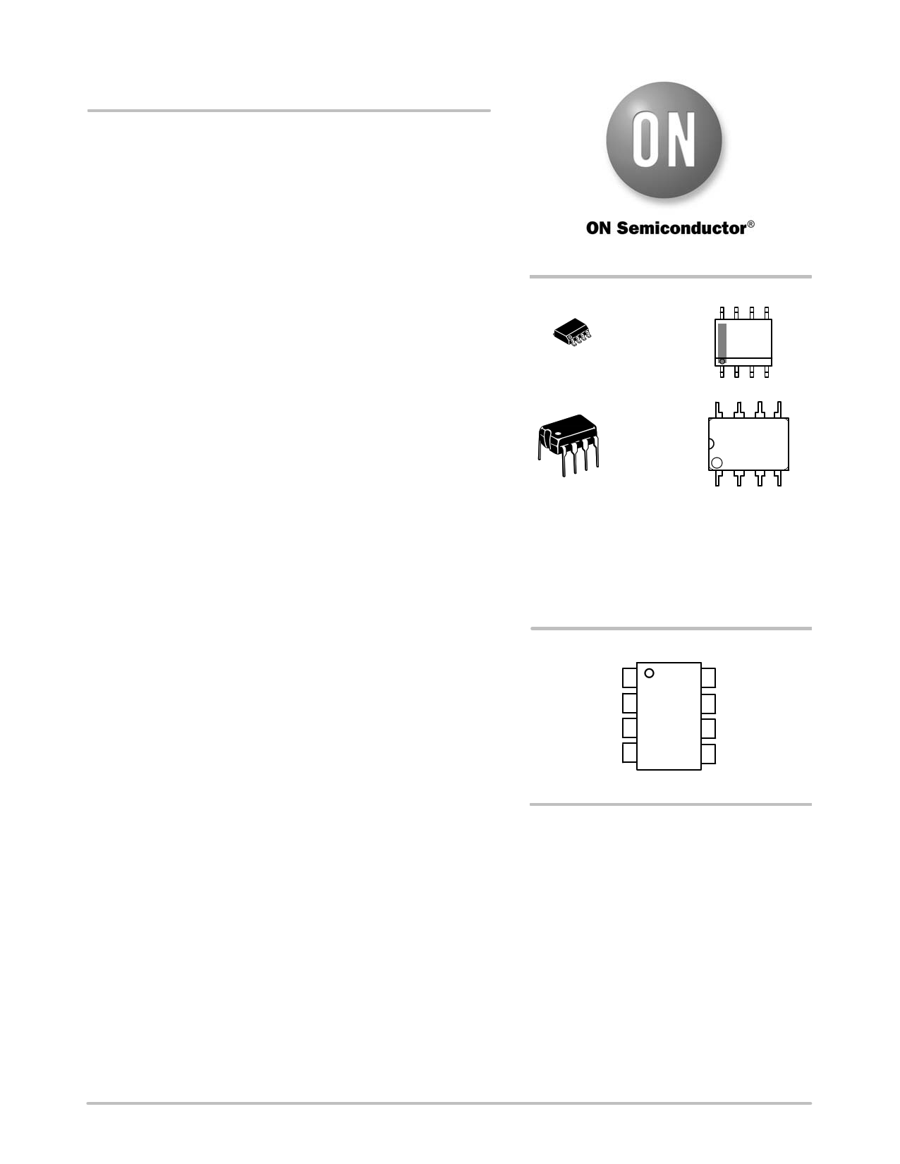
MARKING DIAGRAMS
SOIC-8
D SUFFIX
CASE 751
8
1351x
ALYW
G
1
8
1
PDIP-8
P SUFFIX
CASE 626
NCP1351x
AWL
YYWWG
1
x = A, B, C, or D Options
A = Assembly Location
L, WL = Wafer Lot
Y, YY = Year
W, WW = Work Week
G or G = Pb-Free Package
(Note: Microdot may be in either location)
PIN CONNECTIONS
FB 1
Ct 2
8 TIMER
7 LATCH
Features
•ăQuasi-fixed TON, Variable TOFF Current Mode Control
•ăExtremely Low Current Consumption at Startup
•ăPeak Current Compression Reduces Transformer Noise
•ăPrimary or Secondary Side Regulation
•ăDedicated Latch Input for OTP, OVP
•ăProgrammable Current Sense Resistor Peak Voltage
•ăNatural Frequency Dithering for Improved EMI Signature
•ăEasy External Over Power Protection (OPP)
•ăUndervoltage Lockout
•ăVery Low Standby Power via Off-time Expansion
•ăSOIC-8 Package
• Standard Overcurrent Protection, Latched or
Auto-Recovery, A & B Versions
• Dual Trip Point Overcurrent Protection, Latched or
Auto-Recovery, C & D Versions
• These are Pb-Free Devices
CS 3
GND 4
6 VCC
5 DRV
(Top View)
ORDERING INFORMATION
See detailed ordering and shipping information in the package
dimensions section on page 25 of this data sheet.
Typical Applications
• Auxiliary Power Supply
• Printer, Game Stations, Low-Cost Adapters
• Off-line Battery Charger
©Ă Semiconductor Components Industries, LLC, 2007
November, 2007 - Rev. 3
1
Publication Order Number:
NCP1351/D
1 page 
NCP1351
VDD
FB
VDD
40 mA
ICt
Ct
+
+-
VFault
45k
VDD
ICS-dif*
VOFFset
+
1 ms
Pulse
20 ms Filter
VTIMER
+
VDD
ITIMER
UVLO Reset
Fault = Low
TIMER
DQ
CLK
IP Flag
20 ms Filter
S
Q
Q
R
4V Reset
UVLO Reset
+
VLATCH
VDD
VCC
Mngt
VCCSTOP
1 = OK
0 = not OK
VZENER
Clamp
LATCH
VCC
ICS-dif*
CS
ICS-min*
S
Q
Q
R
DRV
GND
-
+
+
Vth
*(ICS-diff = ICS-max -ICS-min)
Figure 4. C Version (Latched Short-Circuit Protection)
http://onsemi.com
5
5 Page 
NCP1351
Current Sense Pin
Current Sense Resistor
Figure 8. The Voltage on the Current Sense Pin
Below are a few recommendations concerning the wiring
and the PCB layout:
• A small 22 pF capacitor can be placed between the CS
pin and the controller ground. Place it as close as
possible to the controller.
• Do not place the offset resistor in the vicinity of the
sense element, but put it close to the controller as well.
• Regulation by frequency
• The power a flyback converter can deliver relates to the
energy stored in the primary inductance Lp and obeys
the following formulae:
Pout_DCM
+
1ā
2
LPāIpeak2āFSWāh
(eq. 5)
Pout_CCM + 12āLP(Ipeak2 * Ivalley2)FSWāh (eq. 6)
Where:
h (eta) is the converter efficiency
Ipeak is the peak inductor current reached at the on time
termination
Ivalley represents the current at the end of the off time. It
equals zero in DCM.
FSW is the operating frequency.
Thus, to control the delivered power, we can either play on
the peak current setpoint (classical peak current mode
control) or adjust the switching frequency by keeping the
peak current constant. We have chosen the second scheme
Figure 9. The Voltage Across the Sense
Resistor
in this NCP1351 for simplicity and ease of implementation.
Thus, once the peak current has been selected, the feedback
loop automatically reacts to satisfy Equations 5 and 6. The
external capacitor that you connect between pin 2 and
ground (again, place it close to the controller pins) sets the
maximum frequency you authorize the converter to operate
up to. Normalized values for this timing capacitor are
270 pF (65 kHz) and 180 pF (100 kHz). Of course, different
combinations can be tried to design at higher or lower
frequencies. Please note that changing the capacitor value
does not affect the operating frequency at nominal line and
load conditions. Again, the operating frequency is selected
by the feedback loop to cope with Equations 5 and 6
definitions.
The feedback current controls the frequency by changing
the timing capacitor end of charge voltage, as illustrated by
Figure 10.
The timing capacitor ending voltage can be precisely
computed using the following formula:
VCt + 45ĂkĂ(IFB * 40u) ) 500m
(eq. 7)
Where IFB represents the injected current inside the FB
pin (pin 1). The 40u term corresponds to a 40 mA offset
current purposely placed to force a minimum current
injection when the loop is closed. This allows the controller
to detect a short-circuit condition as the feedback current
drops to zero in that condition.
http://onsemi.com
11
11 Page | ||
| Páginas | Total 27 Páginas | |
| PDF Descargar | [ Datasheet NCP1351.PDF ] | |
Hoja de datos destacado
| Número de pieza | Descripción | Fabricantes |
| NCP1351 | Variable Off Time PWM Controller | ON Semiconductor |
| Número de pieza | Descripción | Fabricantes |
| SLA6805M | High Voltage 3 phase Motor Driver IC. |
Sanken |
| SDC1742 | 12- and 14-Bit Hybrid Synchro / Resolver-to-Digital Converters. |
Analog Devices |
|
DataSheet.es es una pagina web que funciona como un repositorio de manuales o hoja de datos de muchos de los productos más populares, |
| DataSheet.es | 2020 | Privacy Policy | Contacto | Buscar |